HR-MB3
8 – 7
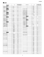
IC400 VHI-1: Li-Ion Charge and Power Manag (BQ24032)
In this unit, the terminal with asterisk mark (*) is (open) terminal which is not connected to the outside.
IC500 RH-IXA069AWZZ: 256MB SDRAM (IXA069AW)
Pin No.
Terminal Name
Input/Output
Function
1
LDO
Output
3.3 V LDO regulator.
2
STAT1
Output
Charge status output1. (open-drain)
3*
STAT2
Output
Charge status output2. (open-drain).
4
AC
Input
Changer input voltage from AC adapter.
5, 6
BAT
Input/Output
Battery input and output.
7
ISET2
Input
Charge current set point for USB port. (High = 500 mA, Low = 100mA) For bp24032 see haif
charge current mode using ISET2.
8
PSEL
Input
Power source selection input. (low for USB, high for AC)
9
CE
Input
Chip enable input. (active high)
10
ISET1
Input/Output
Charge current set point for AC input and precharge and taper set point for both AC and
USB.
11
VSS
—
Ground input (the terminal pad on the underside of the package). There is an internal electri-
cal connection between the exposed thermal pad and VSS pin of the device. The exposed
thermal pad must be connected to the same potential as the VSS pin on the printed circuit
board. Do not used the thermal pad as the primary ground input for the device. VSS pin
must be connected to ground at all times.
12
TS
Input/Output
Temperature sense input.
13
DPPM
Input
Dynamic power path management set point. (account for scale factor)
14
TMR
Input/Output
Timer program input.
15~17
OUT
Output
Output terminal to the system.
18*
ACPG
Output
AC powergood status output. (open-drain)
19*
USBPG
Output
USB powergood status output. (open-drain)
20
IUSB
Input
USB charge input voltage.
Pin No.
Terminal Name
Function
1
VDD
Power supply.
2
DQ0
Data inputs/outputs are multiplexed on the same pins.
3
VDDQ
Data output power.
4, 5
DQ1, DQ2
Data inputs/outputs are multiplexed on the same pins.
6
VSSQ
Data output ground.
7, 8
DQ3, DQ4
Data inputs/outputs are multiplexed on the same pins.
9
VDDQ
Data output power.
10, 11
DQ5, DQ6
Data inputs/outputs are multiplexed on the same pins.
12
VSSQ
Data inputs/outputs are multiplexed on the same pins.
13
DQ7
Dynamic power path management set point. (account for scale factor)
14
VDD
Power supply.
15
LDQM
16
WE
Enables write operation and row precharge. Latches data in starting from CAS, WE active.
17
CAS
Latches column addresses on the positive going edge of the CLK with CAS low. Enables column access.
18
RAS
Latches roe addresses on the positive going edge of the CLK with RAS low. Enables row access & pre-
charge.
19
CS
Disables or enables device operation by masking or enabling all inputs except CLK, CKE and DQM.
20, 21
BA0, BA1
Selects bank to be activated during row address latch time. Selects bank for read/write during column
address latch time.
22
A10
Row/column addresses are multiplexed on the same pins. Row address : RA0 - RA12, Column address :
CA0-CA8
23~26
A0-A3
Row/column addresses are multiplexed on the same pins. Row address : RA0 - RA12, Column address :
CA0-CA8
27
VDD
Power supply.
28
VSS
Ground.
29~34
A4~A9
Row/column addresses are multiplexed on the same pins. Row address : RA0 - RA12, Column address :
CA0-CA8
35, 36
A11, A12
Row/column addresses are multiplexed on the same pins. Row address : RA0 - RA12, Column address :
CA0-CA8
37
CKE
Masks system clock to freeze operation from the next xloxk cycle. CKE should be enabled at least one cycle
prior to new command. Dlsable input buffers for power down in stand-by.
38
CLK
ctive on the positive going edge to sample all input.
39
DQM
Makes data output Hi-Z, tSHZ after the clock and makes the output. blocks data input when DQM active.
Содержание HR-MB3
Страница 13: ...HR MB3 5 4 MEMO ...
Страница 38: ...HR MB3 8 9 MEMO ...


