HR-MB3
8 – 4
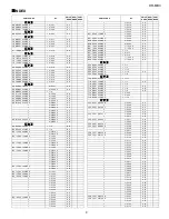
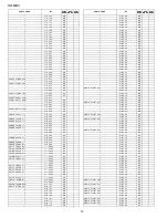
IC201 VHICY68013A-1: USB (CY68013A) (1/2)
In this unit, the terminal with asterisk mark (*) is (open) terminal which is not connected to the outside.
Pin No.
Terminal Name
Input/Output
Function
1
SLRD
Input
SLRD is the input only read strobe with programmable polarity (FIFOPINPOLAR.3) for the
slave FIFOs connected to FD[7..0] or FD[15..0].
2
SLWR
Input
SLWR is the input only read strobe with programmable polarity (FIFOPINPOLAR.2) for the
slave FIFOs connected to FD[7..0] or FD[15..0].
3
AVCC
Input
Analog VCC.
4
XTALOUT
Output
Crystal output.
5
XTALIN
Input
Crystal input.
6
AGND
—
Analog Ground.
7
AVCC
Input
Analog VCC.
8
DPLUS
Input/Output
USB D+Signal.
9
DMINUS
Input/Output
USB D-Signal.
10
AGND
—
Analog Ground.
11
VCC
Input
VCC. Connect to 3.3 V power source.
12
GND
—
Ground.
13*
IFCLK
Output
Interface Clock, used for synchronously clocking data into or out of the slave FIFOs. IFCLK
also servers as a timing reference for all slave FIFO control signals and GPIF. When internal
clocking is used (IFCONFIG.7 =1) the IFCLK pin can be configured to output 30/48 MHz by
bits IFCONFIG.5 and IFCONFIG.6. IFCLK may be inverted, whether internally or externally
sourced, by setting the bit IFCONFIG.4 = 1.
14
Reserved
Input
Reserved. Connect to ground.
15
SCL
Clock for the I2C interface.
16
SDA
Data for I2C-compatible interface.
17
VCC
Input/Output
VCC. Connect to 3.3 V power source.
18
PB0
Input/Output
PB0 is a bidirectional I/O port pin.
19
PB1
Input/Output
PB1 is a bidirectional I/O port pin.
20
PB2
Input/Output
PB2 is a bidirectional I/O port pin.
21
PB3
Input/Output
PB3 is a bidirectional I/O port pin.
22
PB4
Input/Output
PB4 is a bidirectional I/O port pin.
23
PB5
Input/Output
PB5 is a bidirectional I/O port pin.
24
PB6
Input/Output
PB6 is a bidirectional I/O port pin.
25
PB7
Input/Output
PB7 is a bidirectional I/O port pin.
26
GND
—
Ground.
27
VCC
Input
VCC. Connect to 3.3 V power source.
28
GND
—
Ground.
29
CTL0
Output
CTL0 is a GPIF control output.
30
CTL1
Output
CTL1 is a GPIF control output.
31
CTL2
Output
CTL2 is a GPIF control output.
32
VCC
Input
VCC. Connect to 3.3 V power source.
33
PA0
Input
PA0 is bidirectional I/O port pin.
34
PA1
Input
PA1 is bidirectional I/O port pin.
35
SLOE
Input/Output
SOLE is an input only output enable with program-mable polarity (FIFOPINPOLAR.4) for the
slave FIFOs connected to FD[7..0] or FD[15..0]
36
WU2
Input/Output
WU2 is an alternate source for USB Wakeup, enabled by WU2EN bit (WAKEUP.1) and
polarity set by WU2POL (WAKEUP.4).If the 8051 is in suspend and WU2EN = 1, a transition
on this pin starts up the oscillator and interrupts the 8051 to allow it to exit the suspend
mode. Asserting this pin inhibits the chip from suspending, if WU2EN=1.
37
FIFOADR0
Input/Output
FIFOADR0 is an input only address select for the slave FIFOs connected to FD[7..0] or
FD[15..0].
38
FIFOADR1
Input/Output
FIFOADR1 is an input only address select for the slave FIFOs connected to FD[7..0] or
FD[15..0].
39
PKTEND
Input
PKTEND isi an input used to commit the FIFO packet data to the endpoint and whose polar-
ity is program-mable via FIFOPINPOLAR.5.
40
SLCS#
Input
SLCS# gates all other slave FIFO enable/strobes.
41
GND
—
Ground.
42
RESET#
Input
Active low reset.
43
VCC
Input
VCC. Connect to 3.3 V power source
44
WAKEUP
Input
USB wakeup.
45
PD0
Input/Output
Multiplexed pin whose function is selected by the IFCONFIG[1..0] and EPxFIFOCFG.0
(wordwids) bits.
46
PD1
Input/Output
Multiplexed pin whose function is selected by the IFCONFIG[1..0] and EPxFIFOCFG.0
(wordwids) bits.
Содержание HR-MB3
Страница 13: ...HR MB3 5 4 MEMO ...
Страница 38: ...HR MB3 8 9 MEMO ...


