LC-42SB45U
44
2.2
U102(LP2996MRX PSOP-8)
General Description
The LP2996 linear regulator is designed to meet the JEDEC SSTL-2 specifications for termination of DDR-SDRAM. The device contains a high-speed
operational amplifier to provide excellent response to load transients. The output stage prevents shoot through while delivering 1.5A continuous current
and transient peaks up to 3A in the application as required for DDR-SDRAM termination. The LP2996 also incorporates a V
SENSE
pin to provide superior
load regulation and a V
REF
output as a reference for the chipset and DIMMs. An additional feature found on the LP2996 is an active low shutdown (SD) pin
that provides Suspend To RAM (STR) functionality. When SD is pulled low the V
TT
output will tri-state providing a high impedance output, but, V
REF
will
remain active. A power savings advantage can be obtained in this mode through lower quiescent current.
Features
·
Source and sink current
·
Low output voltage offset
·
No external resistors required
·
Linear topology
·
Suspend to Ram (STR) functionality
·
Low external component count
·
Thermal Shutdown
·
Available in SO-8, PSOP-8 or LLP-16 packages
Applications
·
DDR-I and DDR-II Termination Voltage
·
SSTL-2 and SSTL-3 Termination
·
HSTL Termination
23
.U103/ U104 (L5985 VFQFPN8)
Description
The L5985 is a step down switching regulator with 2.5A current limited embedded power MOSFET, so it is able to deliver up to 2A DC current to the load
depending on the application condition.
The input voltage can range from 2.9V to 18V, while the output voltage can be set starting from 0.6V to V
IN
. Having a minimum input voltage of 2.9V, the
device is suitable for buses staring from for 3.3V bus.
Requiring a minimum set of external components, the device includes an internal 250KHz switching frequency oscillator that can be externally adjusted up
to 1MHz.
The QFN package with exposed pad allows reducing the R
thJA
down to approximately 60°C/W.
Features
·
2A DC output current
·
2.9V to 18V input voltage
·
Output voltage adjustable from 0.6V
·
250KHz switching frequency, programmable up to 1MHz
·
Internal Soft-start and Inhibit
·
Low dropout operation: 100% duty cycle
·
Voltage feed-forward
·
Zero load current operation
·
Over current and thermal protection
·
VQFN3x3-8L package
Applications
·
Consumer:
STB, DVD, DVD recorder, car audio, LCD TV and monitors
·
Industrial:
Chargers, car battery, PLD, PLA, FPGA
·
Networking: XDSL, modems, DC-DC modules
·
Computer:
Optical storage, hard disk drive, printers, audio/graphic cards
2
.4. U351/U352 (HYB18TC256160BF-3S TFBGA-84-55)
Features
The 256-Mbit Double-Data-Rate-Two SDRAM offers the following key features:
·
1.8 V
±
0.1 V Power Supply
·
1.8 V
±
0.1 V (SSTL_18) compatible I/O
·
DRAM organizations with 4, 8 and 16 data in/outputs
·
Double Data Rate architecture: two data transfers per clock cycle four internal banks for concurrent operation
·
Programmable CAS Latency: 3, 4, 5 and 6
·
Programmable Burst Length: 4 and 8
·
Differential clock inputs (CK and CK)
·
Bi-directional, differential data strobes (DQS and DQS) are transmitted / received with data. Edge aligned with read data and center-aligned with write
data.
·
DLL aligns DQ and DQS transitions with clock
·
DQS can be disabled for single-ended data strobe operation
Содержание AQUOS LC-42SB45U
Страница 6: ...LC 42SB45U 6 TV Front view TV Rear view ...
Страница 11: ...2008 03 14 LC 42SB45U 11 3 DIMENSIONS ...
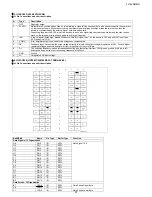
Страница 50: ...LC 42SB45U 50 3 2 U102 LP2996MRX PSOP 8 3 2 1 Pin Connections and short description ...
Страница 54: ...LC 42SB45U 54 3 8 U402 MX25L3205DMI 12G SOP 16 3 8 1 Block Diagram ...
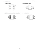
Страница 55: ...2008 03 14 LC 42SB45U 55 3 8 2 PIN CONFIGURATION ...
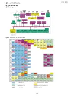
Страница 56: ...LC 42SB45U 56 CHAPTER 6 BLOCK DIAGRAM WIRING DIAGRAM 1 MT5382 POWER MAGAGEMENT BLOCK DIAGRAM ...
Страница 57: ...2008 03 14 LC 42SB45U 57 2 MAIN BOARD BLOCK DIAGRAM ...
Страница 58: ...LC 42SB45U 58 3 WIRING DIAGRAM ...
Страница 59: ...LC 42SB45U CHAPTER 7 PRINTED WIRING BOARD 1 MAIN UNIT PRINTED WIRING BOARD MAIN Unit Side A 59 ...
Страница 60: ...60 LC 42SB45U MAIN Unit Side B ...
Страница 61: ...LC 42SB45U 1 POWER UNIT PRINTED WIRING BOARD POWER Unit Side A 61 ...
Страница 62: ...LC 42SB45U POWER Unit Side B 62 ...
Страница 63: ...LC 42SB45U 63 3 KEY BOARD UNIT PRINTED WIRING BOARD KEY BOARD Unit Side A KEY BOARD Unit Side A ...
Страница 64: ...64 LC 42SB45U IR Unit Side A 3 IR UNIT PRINTED WIRING BOARD IR Unit Side A Cn001 A2 ...
Страница 107: ...2008 03 14 LC 42SB45U 107 2 CABINET PARTS ...


