background image

39


39


   EMC Considerations 


39


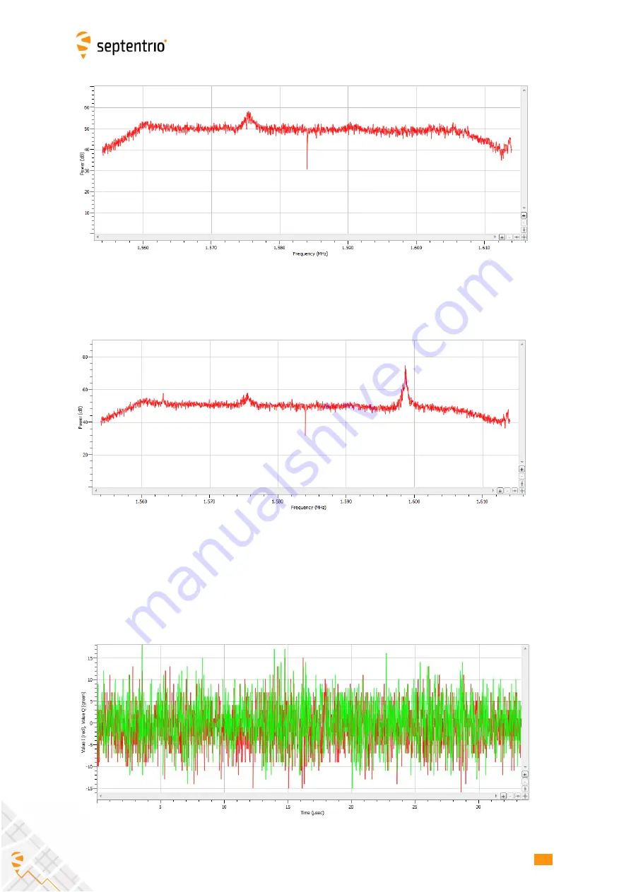
An  example  of  interference  is  shown  below.      This  particular  interference  at  about 
1598 MHz  falls  in  the  GLONASS  L1  band  and  slightly  degrades  the  L1  C/N0  of  some 
GLONASS satellites. 


Try to keep personal computers and other equipment more than 2 meters away from the 
antenna while assessing electromagnetic compatibility of the integration. 
 
RxControl  also  allows  to  observe  the  time  domain  signal.    This  should  look  like  white 
Gaussian noise as illustrated below.   


Содержание mosaic-X5

Страница 1: ...mosaic X5 Hardware Manual Version 1 1 0 ...

Страница 2: ...al Version 1 1 0 October 28 2019 Copyright 2000 2019 Septentrio nv sa All rights reserved Septentrio Greenhill Campus Interleuvenlaan 15i 3001 Leuven Belgium http www septentrio com Phone 32 16 300 800 Fax 32 16 221 640 septentrio ...

Страница 3: ...onsumption 9 2 6 Environmental 9 3 PINOUT AND I O DESCRIPTION 10 3 1 Power Supply 11 3 2 Antenna 11 3 2 1 Electrical Specifications 12 3 3 COM Ports 13 3 4 USB Device Interface 14 3 5 Ethernet 14 3 6 SD Memory Card 15 3 7 Clock Frequency Reference 17 3 7 1 Using the internal TCXO 17 3 7 2 Using and external frequency reference 17 3 8 Event TimeSync inputs 18 3 9 PPS output 19 3 10 General Purpose ...

Страница 4: ...24 5 PRODUCT HANDLING 26 5 1 ESD Precautions 26 5 2 Packaging 27 5 3 Part Number 27 5 4 Moisture Sensitivity 27 5 5 Soldering 27 6 DEVELOPMENT KIT 29 6 1 Powering the DevKit 29 6 2 Antenna Connectors 30 6 3 LEDs and General Purpose Output Pins 31 6 4 COM Ports 31 6 5 PPS Out and Event Inputs 32 6 6 Ethernet 33 6 7 USB Dev 33 6 8 USB Host 33 6 9 REF IN 33 6 10 Buttons 33 6 11 SD Card Socket 34 APPE...

Страница 5: ...5 5 5 APPENDIX B SYSTEM NOISE FIGURE AND C N0 37 APPENDIX C EMC CONSIDERATIONS 38 ...

Страница 6: ...to the antenna from the VANT pin The bias control circuit detects overcurrent conditions 150mA and protects the module in case of short circuit See section 3 2 The module can use its internal TCXO as frequency reference but also accepts an external frequency reference on the REF_I pin See section 3 7 Two event timer pins and a PPS output are available 1 8V LVTTL See section 3 8 The module features...

Страница 7: ... pitch 1 27 mm Land diameter 0 6 mm Pin 1 mark The A1 pad is missing Land plating Nickle Gold Array 23 x 23 three outer rows Number of terminals 239 2 3 Absolute Maximum Ratings The following conditions should never be exceeded even momentarily as it may cause permanent damage to the module Parameter Comment Min Max Units VDD_3V3 voltage See 3 1 0 3 3 6 V VDD_BAT voltage See 3 12 0 3 3 6 V VANT vo...

Страница 8: ...urrent 160 210 500 mA VDD_BAT input current 0 03 1 mA USB_VBUS1 input current See 3 4 10 50 mA 1V8_OUT output current 120 mA 2V8_OUT output current 100 mA VANT input current 150 mA 2 4 2 I O Parameter Comment Min Typ Max Units VIH 1 8V inputs 0 7 1V8_OUT V VIL 1 8V inputs 0 3 1V8_OUT V Input capacitance 1 8V inputs 2 0 pF Pull down 1 8V inputs 80 210 515 kOhm VOH 1 8V outputs 7 2 mA 0 75 1V8_OUT V...

Страница 9: ...t mA GPS L1 C A Stand Alone 1Hz 550 167 GPS L1 L2 RTK 1Hz 670 203 GPS GLONASS L1 L2 RTK 1Hz 695 211 GPS GLONASS L1 L2 GALILEO L1 E5a BeiDou B1C B2a phase 3 RTK 1Hz 850 258 GPS GLONASS L1 L2 GALILEO L1 E5a BeiDou B1C B2a phase 3 RTK 100 Hz 930 282 GPS GLONASS L1 L2 L band PPP 1Hz 760 230 All signals from all GNSS constellations Static 1Hz 910 276 All signals from all GNSS constellations L band Stat...

Страница 10: ...dule provides 239 LGA pads configured as follows The following sections describe all the non reserved pads Pads are grouped by functions Conventions Pin Type I Input O Output P Power Ctrl Control Clk Reference clock PU pulled up PD pulled down K keeper input type TOP VIEW ...

Страница 11: ...e 1V8_LVTTL signals EVENT and PPS see for example section 3 8 The module can also control an external power switch to enable standby mode See section 3 12 for details 3 2 Antenna The antenna can be directly connected to the ANT pad The ANT input is ESD protected in the module and carries a DC voltage to power the antenna avoiding the need for an external bias tee This DC voltage is imposed to the ...

Страница 12: ...th 25 dB net pre amplification 26 dB with 35 dB net pre amplification 35 dB with 45 dB net pre amplification RF nominal input impedance 50 Ohms VSWR 2 1 in 1165 1255 MHz and 1525 1610 MHz range 1 The net gain is the total pre amplification of the distribution network in front of the module Typically this equals antenna active LNA gain minus coax losses in the applicable GNSS bands 2 The listed noi...

Страница 13: ...ive data from the module TXD3 O 3V3_LVTTL Serial COM3 transmit line inactive state is high RXD3 I PU 3V3_LVTTL Serial COM3 receive line inactive state is high RTS3 O 3V3_LVTTL Serial COM3 RTS line The module drives this pin low when ready to receive data CTS3 I PU 3V3_LVTTL Serial COM3 CTS line Must be driven low when ready to receive data from the module TXD4 O 3V3_LVTTL Serial COM4 transmit line...

Страница 14: ...L from Murata 3 5 Ethernet The module supports full duplex 10 100 Base T Ethernet communication The Ethernet PHY and magnetics are to be implemented on the host board Connection with the PHY is through the RMII interface available on the following pins Pin Name Type Level Description Comment RMII_CLK O 3V3_LVTTL LAN PHY Clock MDIO I O 3V3_LVTTL LAN PHY control data MDC O 3V3_LVTTL LAN PHY control ...

Страница 15: ...module can interface to an external SD memory card through the pins listed in the table below Pin Name Type Level Description Comment SD_CLK O 3V3_LVTTL SD card CLK line SD_CMD O 3V3_LVTTL SD card CMD line SD_DAT0 I O 3V3_LVTTL SD card DAT0 line LOGBUTTON I PU 3V3_LVTTL Toggle logging on off or mount unmount the disk See below The module supports the 1 bit SD transfer mode with 3V3 signaling An ex...

Страница 16: ... a 1 10 kOhm series resistor with the switch to protect the module from voltage spikes See instructions in the Reference Guide for details on how to configure SD card logging The module is compatible with SD cards of up to 32GB The file system is FAT32 When powering off the module while logging the last seconds of data may be lost To avoid data losses it is advised to first unmount the SD card Thi...

Страница 17: ... those pins are next to each other 2V8_IN must be connected to 2V8_OUT those pins are next to each other Do not use another 2 8V supply than the one from the 2V8_OUT pin The 10 MHz signal from the internal TCXO is available at the REF_O pin with peak to peak amplitude of 1 2V The waveform is illustrated in the oscilloscope screen capture below 3 7 2 Using and external frequency reference To use an...

Страница 18: ...events on the same EVENTx pin must be at least 5ms and there must be no more than 20 events in any interval of 100ms all EVENTx pins considered If the TimeSync permission is enabled the event inputs can also be configured as TimeSync source using the setTimeSyncSource command When an event pin is configured as TimeSync source the mosaic X5 expects to see a one pulse per second 1PPS signal on that ...

Страница 19: ...mpedant while the module is starting up It finally gets driven to the intended level low or high depending on the user selected PPS polarity after a few seconds If this start up behavior is undesirable it can be shielded by a buffer or level shifter with an output enable The output enable can be controlled with the MODULE_RDY pin of the module The MODULE_RDY signal gets high about 300ms after appl...

Страница 20: ...mple of a circuit with a 10k pull down and a driver is shown below 3 12 Standby The module can control an external power switch allowing for example to toggle between standby and active modes upon pressing an on off push button This functionality involves the following pins Pin Name Type Level Description Comment VDD_3V3 P I 3 3V 5 Main power supply input controlled by the external power switch Al...

Страница 21: ... standby is requested the module terminates all running processes unmounts the disk and drives the PMIC_ON_REQ pin low to turn off the main power supply VDD_3V3 The module power consumption in standby is 5mW When in standby driving the ONOFF pin low for at least 50ms wakes up the module The module restarts in the configuration stored in the boot configuration file The ONOFF pin is internally pulle...

Страница 22: ...is recommended To provide power to the antenna the VANT pins are also connected to the 3 3V supply The antenna is directly fed into the ANT pin The 2V8_IN and 2V8_OUT pins are connected as no external frequency reference is used see section 3 7 The REF_I and REF_O pins are connected for the same reason 1V8_OUT is connected to SYNC this must always be the case All other pins are left unconnected Fo...

Страница 23: ...supply shall be decoupled with at least a 22 µF capacitor with proper voltage rating The other supply terminals don t need external decoupling 4 4 Layout Recommendations 4 4 1 Coplanarity It is important to avoid warpage of the motherboard on which the module will be soldered More in particular Use a symmetrical layer stack Make sure layers opposite from the center of the board have a similar amou...

Страница 24: ...oduce harmful harmonics at GNSS frequencies 1155 1300 MHz and 1540 1610 MHz It is best to keep the antenna input connection short to reduce the area in which signals can be picked up Stitching vias at the input trace could be arranged as a via fence to shield it from interference Furthermore it is important to avoid digital signals in the MHz range SDIO RMII MDIO from running close to the antenna ...

Страница 25: ...tronics on the motherboard like memory busses and clock signals They should also be routed in an inner layer flanked with cupper pours connected to ground Large processor and memory chips sometimes already radiate via the bondwires inside their package Connectors like SD card sockets and radio module sockets also tend to radiate It s best to put these components at the side of the board facing awa...

Страница 26: ... personnel and equipment from electrostatic discharge Handling Remove static sensitive components and assemblies from their static shielding bags only at static safe workstations a properly grounded table and grounded floor mat and only when you are wearing a grounded wrist strap with a resistor of at least 1 mega ohm in series or other grounding device Avoid having non ESD safe material on the wo...

Страница 27: ...red on JEDEC CO 029AN 9x3 matrix trays with 27 modules per tray 5 3 Part Number Mosaic X5 ordering code 410322 5 4 Moisture Sensitivity The moisture sensitivity level MSL is 3 5 5 Soldering Reflow soldering is the soldering method recommended to assemble mosaic X5 modules The recommended temperature profile is specified with the graphic below Refer also to IPC 7530A Guidelines for Temperature Prof...

Страница 28: ...opardize bonding A stencil thickness of 0 1 mm 4 mil is recommended Mount the part with the largest available placement nozzle attached to the center of the shield Use the slowest possible speed of the pick and place machine Preferably place mosaic X5 as the last component on the board If the motherboard thickness is 1 2 mm or less it is recommended to support the assembly during the reflow proces...

Страница 29: ... USB Dev connector J205 This allows powering the board from a PC or from a standard phone charger adapter The supported USB voltage range is 4 5V 5 5V 2 Using the POWER connector J203 The supported voltage range is 5 36V When powering from the USB Dev connector it is recommended to use the USB cable provided with the DevKit Low quality USB cables often suffer from excessive voltage drop preventing...

Страница 30: ... flowing between the two pins and multiply it by 3 3V to obtain the power consumption It is recommended to set the multimeter in high ampere setting to keep the voltage drop as low as possible 6 2 Antenna Connectors There is no antenna connector on the DevKit The antenna must be connected directly to the u FL or MMCX antenna connector on the mosaic X5 interface board The DC voltage 5V or 3 3V at t...

Страница 31: ... The 3 3V GP1 and GP2 outputs are available on the J501 header 6 4 COM Ports By default the four COM ports of the mosaic X5 module are routed to the four DB9 connectors of the DevKit Electrical levels on the BD9 conform to the RS232 standard RTS CTS lines are supported only on COM2 and COM3 the mosaic X5 has RTS CTS lines on COM1 as well but they are not routed to the DevKit Connection to a PC is ...

Страница 32: ... pin header The other COM ports are still routed to the DB9 connectors using the RS232 levels 6 5 PPS Out and Event Inputs The PPSout pin of header J500 is connected to the PPSOUT pin of the mosaic X5 module through a 1 8V to 3 3V level shifter The PPS level at the header is 3 3V The EVENTA and EVENTB pins of J500 are connected to the EventA and EventB pins of the mosaic X5 through a level shifter...

Страница 33: ...v That connector can be attached to a PC to power the DevKit and to communicate with the module over its USB port 6 8 USB Host Reserved 6 9 REF IN The REF IN SMA connector can be used to feed the module with an external 10 MHz sinusoidial frequency reference Input impedance 50 Input level between 10dBm and 14dBm 0 2Vp p to 3 2Vp p 6 10 Buttons nRST LOGGING GND ...

Страница 34: ...o enabled and disable logging as described in section 3 6 The buttons are also connected to J601 and J602 2 pin headers see above picture Connecting the nRST or LOGGING pins of these headers to ground is the same as pressing the respective button 6 11 SD Card Socket The module can log files on the micro SD Card in this socket See section 3 6 for a description of the SD Card logging on the mosaic X...

Страница 35: ...fferential corrections have been provided in the last received differential correction message RTCM or CMR LED behaviour Number of satellites with corrections LED is off No differential correction message received blinks fast and continuously 10 times per second 0 blinks once then pauses 1 2 blinks twice then pauses 3 4 blinks 3 times then pauses 5 6 blinks 4 times then pauses 7 8 blinks 5 times t...

Страница 36: ...e LOGLED reports the SD card mount status and logging activity LED LED Behaviour LOGLED LED is off when the SD card is not present or not mounted LED is on when the SD card is present and mounted Short blinks indicate logging activity ...

Страница 37: ...5dB 15dB and NRrx is 8 5dB see table in section 3 2 In this case the system noise figure is NFsys 10 log10 102 5 10 108 5 10 1 1015 10 2 95 dB The C N0 in dB Hz of a GNSS signal received at a power P can be computed by C N0 P 10 log10 Tant 290 10NFsys 10 1 228 6 dB where P is the received GNSS signal power including the gain of the antenna passive radiating element in dBW e g 155dBW Tant is the an...

Страница 38: ...ns the C N0 values should reach up to 50 dB Hz for the strong signals on L1 and L5 and up to 45 dB Hz on L2 as illustrated below If the maximum C N0 is lower than expected interference and cross talk from nearby electronics is likely and the source of the problem needs to be identified This is where the RF spectrum monitor built in the GNSS receiver comes in handy The spectrum monitor can be acces...

Страница 39: ...band and slightly degrades the L1 C N0 of some GLONASS satellites Try to keep personal computers and other equipment more than 2 meters away from the antenna while assessing electromagnetic compatibility of the integration RxControl also allows to observe the time domain signal This should look like white Gaussian noise as illustrated below ...

Страница 40: ... system frequencies For example peaks at 1200 and 1248 MHz are an indication of an interfering source at 48 MHz as this maps to the 25th and 26th harmonic of a 48 MHz signal This may correspond to the frequency of a microcontroller in the application Integration cross talk can be solved in a number of ways Shift the clock frequency of the interfering signal to avoid the GNSS bands Use shielding ta...

Отзывы: