background image


© by SEMIKRON  

/  2017-09-07  /  

Technical Explanation

  /  SKiiP

®

4


Page 44/73

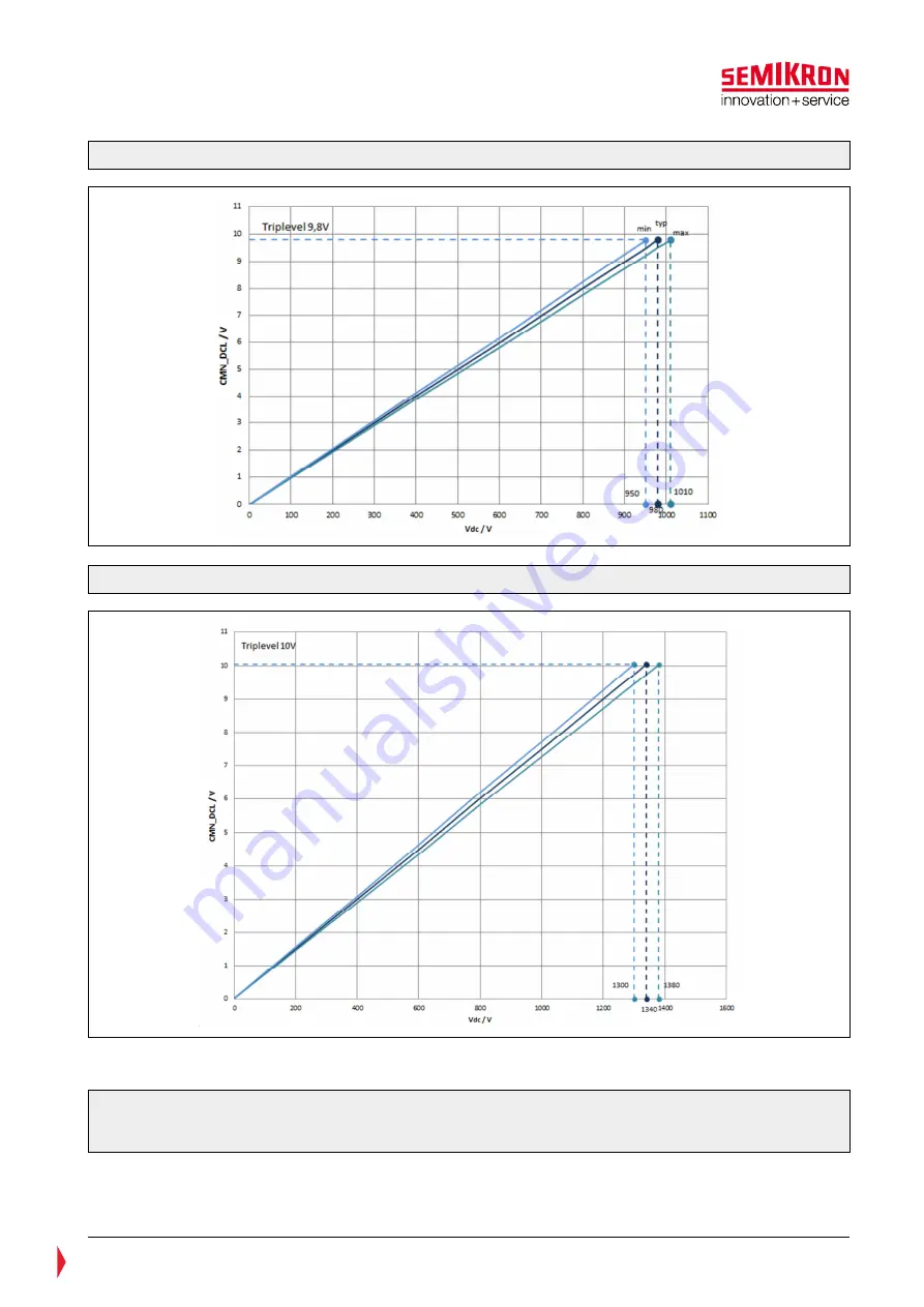
Figure 5.32: DC link voltage sensor output 1200V system 


Figure 5.33: DC-link voltage sensor output 1700V system 


The value f

0Uana

 =1,8kHz is marked in Figure 5.34. 


Please note:

 The SKiiP

®

4 for 1500V photovoltaic applications do not protect against an DC-link 

overvoltage. The user must take care of keeping the DC-link voltage within suitable limits in the 
application.  


Содержание 20601123

Страница 1: ...DUW 20601236 SKiiP 2414 GB17E4 4DUW 20602036 SKiiP 2414 GB17E4 4DUW 20601137 SKiiP 3614 GB12E4 6DUW 20602037 SKiiP 3614 GB12E4 6DUW 20601238 SKiiP 3614 GB17E4 6DUW 20602038 SKiiP 3614 GB17E4 6DUW 20601139 SKiiP 1814 GB12E4 3DUL 20602039 SKiiP 1814 GB12E4 3DUL 20601240 SKiiP 1814 GB17E4 3DUL 20602040 SKiiP 1814 GB17E4 3DUL 20601141 SKiiP 2414 GB12E4 4DUL 20602041 SKiiP 2414 GB12E4 4DUL 20601242 SKi...

Страница 2: ...ctive earth chassis connection 29 5 2 11 Reserved or not used signals 30 5 3 Gate driver board 31 5 3 1 Overview 31 5 3 2 Digital signal transmission 31 5 3 3 Power On Reset 31 5 3 4 Interlock Dead Time Generation 32 5 3 5 Short pulse suppression 32 5 3 6 IntelliOff 33 5 3 7 Error Management 35 5 3 8 Analogue signals sensor functionality 38 6 Power terminals 46 6 1 Electrical limits 46 6 2 Mechani...

Страница 3: ... Page 3 73 7 12 Prevention of condensation 65 8 Logistics 66 8 1 Label 66 8 1 1 System Label 66 8 1 2 Half bridge Laser Label 67 8 1 3 Warranty Label 67 8 1 4 Data Matrix Code 67 8 1 5 Provisions and handling after use 68 9 Abbreviations 71 10 Symbols 72 ...

Страница 4: ...rface SKiiP 4 CANopen User Manual Diagnostic Interface SKiiP 4 CANopen Object Dictionary Technical Explanation SKiiP 4 Parallel Board Technical Explanation SKiiP 4 F Option Technical Explanation SKiFace Adapter Board All these documents can be found on the SEMIKRON internet page www semikron com or requested at SEMIKRON ...

Страница 5: ...ink power stage gate drive and protection circuitry Figure 2 1 SKiiP 4 4 fold The power section consists of 3 4 or 6 parallel connected half bridge modules whereas a half bridge is defined in Figure 2 2 The exploded assembly view of a half bridge module is shown in Figure 2 3 and as convention the IGBT and the diode connected between DC and AC are named TOP IGBT and TOP diode respectively Conseque...

Страница 6: ...refer to the PI 12 034 for such detailed information and get in touch with your local SEMIKRON representative in case further assistance is required 2 2 Power section The SKiiP 4 power section is constructed utilizing pressure contact technology and without a copper base plate e g the SKiiP 4 is a baseplateless module Thus the pressure to attach the substrate to the heatsink is homogenously induce...

Страница 7: ...sed for all connections between substrate and Gate Driver PCB like for the gate auxiliary emitter and temperature sensor These spring contacts allow the solder free connection of the driver board 2 3 Gate Drive Unit The Gate Driver Unit controls the behavior of the SKiiP under normal and exceptional operation It receives checks and conditions the input signals to further transform them into suitab...

Страница 8: ... by SEMIKRON 2017 09 07 Technical Explanation SKiiP 4 Page 8 73 3 Topologies and selection guide 3 1 Type Designation Code ...

Страница 9: ...urrent ratings ICnom Table 3 1 SKiiP 4 standard product range 3 fold 4 fold 6 fold SKiiP 1814GB12E4 3DUW SKiiP 1814GB17E4 3DUW SKiiP 2414GB12E4 4DUW SKiiP 2414GB17E4 4DUW SKiiP 3614GB12E4 6DUW SKiiP 3614GB17E4 6DUW SKiiP 1814GB12E4 3DUL SKiiP 1814GB17E4 3DUL SKiiP 2414GB12E4 4DUL SKiiP 2414GB17E4 4DUL SKiiP 3614GB12E4 6DUL SKiiP 3614GB17E4 6DUL ICnom 1800A ICnom 2400A ICnom 3600A ...

Страница 10: ...Sinusoidal Sweep 5g x y z axis 2h axis IEC 60068 Part 2 6 09 Shock Halt Test Half sinusoidal Pulse 30g x y z direction 1000 times per direction IEC 60068 Part 2 27 10 Corrosive gas test Ta 25 C 75 RH 4 components H2S hydrosulphide NO2 nitrogen dioxide Cl2 Chlorine SO2 Sulphur dioxide 21 days IEC 60068 Part 2 60 4 2 Electromagnetic compatibility EMC The SKiiP 4 is designed to withstand the followin...

Страница 11: ...o 2000m The required clearance distances between mains circuits and their environment for overvoltage category III are listed in EN50178 For an earthed neutral system the rated isolation voltage is defined in chapter 5 2 16 1 of EN50178 as the peak value of the rated voltage between phase and earthed neutral point Based on this standard sentence the rated isolation voltage in case of a grounded de...

Страница 12: ...cited standard shall not be reduced The required clearance distances between mains circuits and their environment for overvoltage category II are listed in EN50178 If safety isolation is necessary the maximum altitude of SKiiP 4 is 6250 m 690 TN grid and overvoltage category II If only basic isolation is required even higher operation altitudes are possible In case of a 690V TN grid and overvoltag...

Страница 13: ... between SKiiP 4 driver interface and controller board Finally the installation altitude of the SKiiP 4 depends on Grid configuration star grounded grid delta grounded grid The voltage level of the line to earth voltage rated isolation voltage The overvoltage category II or III Whether safety isolation is required or not ...

Страница 14: ... Grounded delta grid TN 690V Basic isolation against ground Required for 2000m 8 mm 5 5 mm 5 5 mm 3 mm Existing 8 mm Factor 1 1 45 1 45 2 66 Altitude 2000m 4840m 4840m 9000m Rein forced isolation Required for 2000m 14 mm 8 mm 14mm 8mm Existing 14 mm Factor 1 1 75 1 1 75 Altitude 2000m 6250m 2000m 6250m Maximum Altitude with safety isolation 2000m 4840m 2000m 6250m Maximum Altitude without safety i...

Страница 15: ...view The functionality of the Gate Driver board is indicated in the following block diagram Gate driver interface SKiFace marked as red block in Figure 5 1 refer to Chapter 5 2 Gate driver board marked as green block in Figure 5 1 refer to Chapter 5 3 Figure 5 1 Gate Driver Board block diagram ...

Страница 16: ...refer to chapter 5 2 3 Switching signal input refer to chapter 5 2 4 Analogue signals refer to chapter 5 2 5 HALT logic refer to chapter 5 2 6 CMN_GPIO 1 output refer to chapter 5 2 7 CMN_GPIO 2 refer to chapter 5 3 6 CAN interface refer to chapter 5 2 8 Figure 5 2 Gate Driver Interface Figure 5 3 SKiiP 4 connector D Sub 25 pin male plug vertical top view Picture Pin Configuration Dimensions When ...

Страница 17: ... to operate e g error HIGH recessive ready to operate For details refer to HALT Logic Signal p 24 6 CMN_TEMP Temperature signal out This pin is used to indicate the temperature sensor s analogue signal Max output current 5mA Nominal voltage range 0 10V Refer to Integrated DCB Temperature Sensor p 42 7 CMN_DCL DC Link voltage out This pin is used to indicate the DC Link voltage level Max output cur...

Страница 18: ...GPIO1 signal p 26 19 CMN_TEMP_GND Ground for CMN_TEMP 20 CMN_DCL_GND Ground for CMN_DCL 21 HB_BOT Switching signal input for low side IGBT LOW Low side IGBT off HIGH Low side IGBT on For details refer to Switching Signal Inputs p 21 22 HB_GND Ground for CMN_HB_TOP CMN_HB_BOT CMN_HB_RSRVD Internally connected to PWR_GND 23 HB_I_GND Ground for HB_I 24 CAN_L CAN interface INPUT OUTPUT LOW Input imped...

Страница 19: ...Switching signal BOT Chassis PE 14 17 22 1 2 3 6 19 7 20 23 10 8 21 SKiiP 4 Driver interface SKiFace Controller interface GND Analogue output Digital input Digital output Digital output GND GND GND GND Analogue input VS PWR_GND CMN_GND HB_GND PWR_VS Supply voltage GND DC DC SHLD_GND 13 D Sub cable shield Capacitive grounding direct grounding 24V 0V External power supply RXD TXD CAN_H CAN_L RXD TXD...

Страница 20: ...ufficient margin in case of overload it is recommended to select the rated current of the external power supply sufficiently higher than the SKiiP s maximum specified input current see symbol Is on page 2 of the corresponding SKiiP 4 datasheet If the power supply is able to provide a higher current a peak current will flow in the first instant to mainly charge the input capacitances on the driver ...

Страница 21: ... input will be considered as LOW signal Figure 5 5 TOP BOT PWM Signal Input A 1nF capacitor is connected to the switching signal input to obtain high noise immunity This capacitor can cause a delay of few ns for current limited line drivers which can be neglected Input resistance is about 13kOhm As shown in Figure 5 7 the switching signal will be considered as High when VIT Low when VIT Figure 5 6...

Страница 22: ... short circuit at the analogue output Please ensure that the maximum current driven by the output of the operational amplifier does not exceed 5mA A common mode choke and 100pF capacitors are used on the outputs to obtain high noise immunity On the user controller board a differential amplifier should be used which is connected to the analogue output and the corresponding ground signals CMN_TEMP_G...

Страница 23: ...arallel to the feedback resistor R3 and also not to the resistor of the non inverting input to ground R3 These capacitors have often high tolerances so the common mode rejection of the circuitry is reduced by this effect No capacitor should be connected between the plus and the minus pin of the operational amplifier as well This additional corner frequency can lead to an oscillating signal The inp...

Страница 24: ... application can be connected together Also other hardware components can be connected to this signal when an open drain collector output is implemented In this case all signals that are connected to the HALT signal are wired ored That means the HALT signal is set to LOW state when one of the connected SKiiPs is not ready to operate Please note In this paralleled configuration there is no possibil...

Страница 25: ...onnected in parallel the pull up resistor on the driver board is relatively high 51 1kOhm The pull up resistor on the user controller board should be at least 1kOhm A delay of the HALT signal due to the capacitors on the driver board 10nF must be considered Figure 5 9 Application example of the HALT signal processing for separated SKiiP 4 systems Please note If the HALT signal is not used it must ...

Страница 26: ... further information Please note As the CMN_GPIO1 signal is the inverted HALT signal there is no possibility to see which SKiiP 4 has set the error output signal For this purpose the CAN diagnostic interface should be used Figure 5 10 indicates on the left hand side the output stage of the CMN_GPIO1 signal on the right hand side an example of the input stage of the user controller board for each C...

Страница 27: ...ell as the activation of a dedicated function to ride through extraordinary wind turbine specific application conditions For further details please refer to the FRT function see Chapter 7 7 or DC Link trip level deactivation Please note By deactivating the supervision of VDCtrip the related SKiiP4 data sheet limits must be strictly observed by the user The violation of these limits can lead to the...

Страница 28: ...cal Explanation SKiiP 4 Page 28 73 For a detailed description of the SKiiP4 CAN interface please refer to the following documents Diagnostic Interface SKiiP4 CANopen User Manual Diagnostic Interface SKiiP4 CANopen Object Dictionary ...

Страница 29: ...pply current Driver Board User Controller Board Supply current 5 2 10 Shield and protective earth chassis connection The shield of the D Sub connector is connected to GND at the gate driver board There is no connection at the gate driver board to heat sink nor to any other protective earth connections On the user controller board the shield should be connected to the chassis which is linked to Pro...

Страница 30: ... used signals Unused pins of digital signals CMN_GPIO1 CMN_GPIO2 at the user controller board should be connected to VS by a 51kOhm resistor in series to a diode as shown in Figure 5 16 The diode prevents from supplying the controller from the driver board when the controller is not supplied Also a capacitor should be connected to GND to damp burst signals For the CAN interface it is recommended t...

Страница 31: ...turn off conditions are detected and reduced by the gate driver through an implemented function further called intelligent turn off control circuit 5 3 2 Digital signal transmission The driver board provides two independent signal channels communicating from low voltage to high voltage side to transfer switching and sensor signals The signals are transferred by dedicated pulse transformers which a...

Страница 32: ... as tTD in the SKiiP 4 data sheet The dead time circuit prevents that TOP and BOT IGBT of one half bridge are switched on simultaneously It is allowed to control the SKiiP 4 by inverted pulses e g without controller generated dead time tTD is not added to a dead time provided by the controller see Figure 5 18 5 3 5 Short pulse suppression The short pulse suppression time is defined as tSIS in the ...

Страница 33: ...KiiP 4 has two different gate turn off speeds determined by the internally connected and optimized gate resistors The suitable gate turn off speed will be chosen as a function of the actual measured AC current value As shown in Figure 5 19 there are two different turn off speed scenarios Figure 5 19 Turn off speed scenarios ...

Страница 34: ...In the IntelliOff mode the IGBT is turned off by using higher gate resistors compared to normal turn off Table 5 5 Power loss impact of IntelliOff operation 3GB 4GB 6GB Please note When operating two or more SKiiP 4 modules in parallel connection the GPIO2 port is used to synchronize the IntelliOff mode for widely balanced current sharing when IntelliOff is activated The GPIO2 must be assigned to ...

Страница 35: ...Figure 5 22 Please note The DC link overvoltage monitoring is disabled at 1500V Photovoltaic SKiiP 4 Systems 5 3 7 1 Error delay time td err The error delay time is the propagation delay time of an error This time is different for the different types of errors The precise values for each specific error type can is summarized in Table 5 6 Table 5 6 Error delay time Type of error Typical values DC L...

Страница 36: ... fsw Figure 5 20 illustrates the frequency ranges Figure 5 20 Switching frequency range 5 3 7 4 Overlapping of switching signals It is not allowed that TOP and BOT IGBT of a half bridge are turned on at the same time Such an overlapping condition is observed and in case it persists for minimum 3µs the IGBTs are turned off After the overlapping situation has ended and the interlock time has elapsed...

Страница 37: ... that the peak load current stays safely below the over current protection level For further details please refer to the corresponding datasheet of the SKiiP 4 5 3 7 6 Short Circuit Protection SCP The short circuit protection SCP circuit is protecting against short circuit situations by initiating a safe turn off of the IGBTs The protection circuit monitors the collector emitter voltage VCE of the...

Страница 38: ... variations Consequently the protection function derived from the substrate temperature sensor s temperature needs evaluation under the real application conditions such as peak current load profile etc and suitable protection levels shall be set 5 3 8 Analogue signals sensor functionality 5 3 8 1 Load current sensor Each half bridge module refer to Figure 2 1 has an integrated load current sensor ...

Страница 39: ... by SEMIKRON 2017 09 07 Technical Explanation SKiiP 4 Page 39 73 ...

Страница 40: ...2017 09 07 Technical Explanation SKiiP 4 Page 40 73 Figure 5 27 Characteristic between current and the voltage at HB_I SKiiP 4 4 fold Figure 5 28 Characteristic between current and the voltage at HB_I SKiiP 4 6 fold ...

Страница 41: ...a small coil with a high permeable core Due to the properties of this sensing element there is low gain and linearity failure An electronic circuit evaluates the value of the field sensor and feeds a current into the compensation coil to keep the effective magnetic field at zero The demanded compensation current measured by a burden resistor A measurement circuit generates a voltage that is propor...

Страница 42: ...e analogue temperature signal is available on the SKiFace interface see Table 5 1 with characteristic given below Table 5 9 Characteristics of the DCB temperature sensor circuit Temperature signal characteristics Value Trip level Ttrip 135 C Minimum measurable temperature TMIN 30 C Analogue temperature signal CMN_TEMP 150 C 10V Analogue temperature signal CMN_TEMP 30 C 0V Accuracy of analogue sign...

Страница 43: ...ltage signal is available on the SKiFace interface see Table 5 1 with the characteristic given in Table 5 10 Table 5 10 VDC characteristics VDC signal characteristics 1200V System 1700V System 1500V PV Analogue DC link voltage signal CMN_DCL 900VDC 9V 6 75V 6 3V Analogue DC link voltage signal CMN_DCL 1200VDC 9V 8 4V Voltage ratio 10mV V 7 5mV V 7mV V Accuracy of analogue signal VDCTrip over full ...

Страница 44: ... system Figure 5 33 DC link voltage sensor output 1700V system The value f0Uana 1 8kHz is marked in Figure 5 34 Please note The SKiiP 4 for 1500V photovoltaic applications do not protect against an DC link overvoltage The user must take care of keeping the DC link voltage within suitable limits in the application ...

Страница 45: ... by SEMIKRON 2017 09 07 Technical Explanation SKiiP 4 Page 45 73 Figure 5 34 Bode diagram of the DC link voltage measurement at the SKiiP4 interface ...

Страница 46: ...ection to the terminals but should not exceed a specified torque to limit the mechanical stress to the plastic housing preventing any damage to the plastic body Please refer to the corresponding information contained in the datasheet to adjust the mounting tool accordingly The power terminals of the SKiiP 4 are widely robust against external forces which may be caused by the connection of the DC l...

Страница 47: ...n The terminals must not heat up snubber capacitors Symmetrical layout of DC connection The inductance between the terminals and the DC link capacitor should be equal for a symmetrical current sharing between the half bridges AC connection Symmetrical AC connections for symmetrical current sharing between the paralleled half bridge modules The load cable should be connected in the middle of the AC...

Страница 48: ...017 09 07 Technical Explanation SKiiP 4 Page 48 73 Figure 6 2 AC connection Please note All screws of the AC terminals must be tightened uniformly not one screw completely fixed before the others to avoid the warping ...

Страница 49: ...es which affects the lifetime of the electronics Load and temperature cycles which affect the lifetime of the power part Environmental conditions during operation transport and storage EMC design Mechanical design Cosmic ray robustness evaluation Besides these general points application specific conditions and requirements may be considered too 7 2 Safe Operating Area for SKiiP 4 The principle Saf...

Страница 50: ...it has to be validated by testing that the capacitors are compatible with the design and that they will not be overloaded Table 7 1 Snubber capacitors for SKiiP 4 Capacitance DC voltage For use with 680 nF 1000V 1200V device 330 nF 1600V 1700V device 7 4 Definition of Thermal Resistance The definition of the thermal resistances given in the SKiiP 4 datasheet are shown in the Figure 7 2 Figure 7 2 ...

Страница 51: ...e of the power semiconductors Since the temperature sensor is close to the IGBT and mounted on the substrate the actual and precise IGBT temperature cannot be acquired Consequently the protection function derived from the substrate temperature sensor s temperature needs evaluation under the real application conditions such as peak current load profile etc During operation there will be a temperatu...

Страница 52: ...n in the Figure 7 4 The SKiiP IPM shall be mounted by means of the fixing holes in the side parts ensuring that constructed gap is unsupported The parameters for vibration and shock are given in Table 4 1 In case of usage of M8 screw ISO 4762 strength class 8 8 the torque of 10 12Nm is recommended Regarding the selection of the coolant type the used materials of the cooling circuit need to be cons...

Страница 53: ... 1179 2 G 1 2 A L Fitting ISO 1179 3 G 1 2 A G Fitting ISO 1179 2 G 1 2 A L Fitting of shape E according to ISO 1179 2 with G thread tolerance class A DIN EN ISO 228 L is for lower pressures max 250 bar Sealing with a additional profile sealing ring rubber according to ISO 1179 2 G 1 2 A Dimension of profile sealing ring according to ISO 1179 2 D6 mm 18 5 d7 mm 23 9 L5 mm 1 5 L6 mm 0 8 Figure 7 6 ...

Страница 54: ...g to ISO 1179 3 Stützring mm d10 23 3 d11 28 5 L10 1 9 O Ring mm d8 17 86 d9 2 62 Figure 7 7 Description of fitting ISO 1179 3 G 1 2 A G Fitting according to DIN 3852 2 C R is not recommended only for exceptional cases Please note The given specifications for gaskets of the pipe fittings are recommended values and have to be validated by customer depending on production equipment and application ...

Страница 55: ...nnected However the DUT might be still electrically charged In this case it would be dangerous to touch the DUT after the test procedure In addition to this without grounding the test voltage could drift and the voltage to ground will be even higher than the nominal test voltage All isolation voltage tests must be performed at an ambient temperature of 15 35 C a relative humidity of 45 75 and an a...

Страница 56: ...the longer the voltage stress is applied the stronger the damage of the isolation through the partial discharge will be Thus each IVT leads to a potential weakening of the isolation Partial discharge in the DCB doesn t necessarily lead to a weakening of the isolation because the ceramic substrate tends to be robust against partial discharge First of all organic materials plastic e g circuit boards...

Страница 57: ...d by the SKiiP driver itself regardless of whether the PWM from the customer controller pwmcontroller is running The SKiiP driver sets the CMN_HALT signal to LOW and the CMN_GPIO1 signal to HIGH The interrupt of the pwmSKiiP is released after the error memory reset time tpRESET has elapsed and if the switching input signals HB_TOP and HB_BOT are set to LOW In most cases tpRESET is too high to fulf...

Страница 58: ...nabled to start switching as long as the overcurrent trip level is not exceeded again Figure 7 12 Graphic presentation of the driver processing in FRT case The freewheeling diodes conduct the rotor current Irotor during the period of blocked pwmSKiiP The user must take care that the diodes will not be overloaded thermally because the SKiiP s overcurrent protection is deactivated and the thermal pr...

Страница 59: ...in the Figure 7 13 While the SOA for the standard SKiiP 4 shown in the Figure 7 1 is limited by the over voltage trip level VDCtrip and over current trip level ITRIPSC the modified SOA of the PV SKiiP 4 employs an extended area above VDCtrip and limited by the low load current ILL and a higher over voltage trip level VDCtripLL This operation mode is called solar mode and is marked orange in the ri...

Страница 60: ...of this error both error bits 13 over current and 14 DC Link error will be set Please refer to the CANopen Object Dictionary Rev 6 chapter 3 8 Error recording for more details Suitable snubber capacitors must be used in case the maximum blocking voltage VCES VRRM is exceeded Please refer to chapter 7 6 for further information For safe operation the interlock time tTD is increased to a value 4 5µs ...

Страница 61: ...mise between exploiting the electrical and thermal capability of a device and obtaining an acceptable failure rate and life time expectation The following temperature rating is recommended for the SKiiP4 systems Power section It is necessary to ensure by calculations and measurements that the recommended IGBT and diode junction temperatures are not exceeded at maximum overload conditions stipulate...

Страница 62: ... could be measured by means of a temperature sensor located at the bottom side of the driver PCB see Figure 7 16 The value of the sensor could be read out via CAN bus interface please refer to the CANopen documentation for further information If the temperature exceeds the TDriver Trip given in the SKiiP 4 s data sheet the switching operation will be blocked and an error signal will be issued corr...

Страница 63: ...ecommended AC connection is shown in Figure 7 17 The current sharing should be measured in the design phase by double pulse testing see AN 7006 and in the final design under real operation conditions This can be done e g by Rogowski current sensors which are located around the DC and DC terminals 7 11 Paralleling of SKiiP 4 The parallel operation of SKiiP 4 s requires the following considerations ...

Страница 64: ... inductance between the AC output terminals of the paralleled SKiiP subsystems The impedance has two tasks On one hand it should prevent from the generation of an imbalance current during the switching moment That could lead to different switching loss and in severe cases to undesired oscillations This is shown in Figure 7 18 The value tjitter is given in the SKiiP 4 data sheet on page 2 Figure 7 ...

Страница 65: ...mentioned actions it has to be taken into account that for remaining imbalanced current sharing a derating of the nominal current of the power stage has to be considered Different production lot In general besides all the before mentioned constraints it is not recommendable although not impossible to parallel SKiiP4 of different production lots Typically the relevant parameters for an advantageous...

Страница 66: ...arked with a system half bridge driver shuttle and a warranty label 8 1 1 System Label The system label of the SKiiP Figure 8 1 contains all information necessary for customers to clearly identify the product In case of technical inquiries please always refer to the SKiiP Item number written on this label Figure 8 1 System Label of SKiiP 4 ...

Страница 67: ... note Removing the warranty label will result in loss of warranty in case of product reclamation 8 1 4 Data Matrix Code The Data Matrix Code is described as follows Cell size 0 3mm Read distance 60 100mm Max angle of 30 vertical reference line for reading Figure 8 4 Data Matrix Code of SKiiP 4 example 2060XXXX01_16DE12345601_001_ABCDEFGHIJ 10 digits free for customer information 3 digits continuou...

Страница 68: ... by SEMIKRON 2017 09 07 Technical Explanation SKiiP 4 Page 68 73 8 1 5 Provisions and handling after use Components which are obsolete or defective must be disposed according to local regulations ...

Страница 69: ...n off speed scenarios 33 Figure 5 20 Switching frequency range 36 Figure 5 21 Timing diagram for the TOP BOT overlapping error processing t 3µs 36 Figure 5 22 Timing diagram for the HB_TOP HB_BOT overlapping error processing t 3µs 37 Figure 5 23 No short circuit 38 Figure 5 24 Short circuit during operation 38 Figure 5 25 Short circuit during turn on 38 Figure 5 26 Characteristics between current ...

Страница 70: ... 4 Electromagnetic compatibility 10 Table 4 3 Isolation limits SKiiP 4 11 Table 4 4 Altitude correction factors IEC 60664 1 12 Table 4 5 Installation altitudes for SKiiP 4 as function of the grid configuration overvoltage category and required isolation degree 14 Table 5 1 Pin configuration SKiiP 4 17 Table 5 2 Requirements to the auxiliary power supply 20 Table 5 3 Ground connections of SKiiP 4 2...

Страница 71: ...ugh FwDi Free wheeling diode GB halfbridge configuration GND Ground IGBT Insulated Gate Bipolar Transistor IPM Intelligent Power Module IVT Isolation Voltage Test PCB Printed Circuit Board PTC Positive Temperature Coefficent RH Relative Humidity RoHS Restriction of Hazardous Substances SCP Short Circuit Protection SKiiP Semikron intelligent integrated Power SPS Short Pulse Suppression UVP Under Vo...

Страница 72: ... tjitter Jitter clock time tSIS Short pulse suppression time tbl Blanking time tPOR Power On Reset time Ta Ambient temperature Tj Junction temperature Tr Temperature at reference position ULE Line to earth voltage ULL Line to line voltage VCEstat Collector Emitter Threshold Static Monitoring Voltage Vit HALT Input threshold voltage HALT signal HIGH Vit HALT Input threshold voltage HALT signal LOW ...

Страница 73: ...e Tj Junction temperature Tr Temperature at reference position ULE Line to earth voltage ULL Line to line voltage VCestat Collector Emitter Threshold Static Monitoring Voltage Vit HALT Input threshold voltage HALT signal HIGH Vit HALT Input threshold voltage HALT signal LOW TDriverTrip Over temperature trip level f0Uana Bandwidth of DC voltage measurement VDctrip f0Iana Bandwidth of current measur...

Отзывы: