-10-
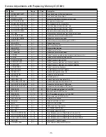
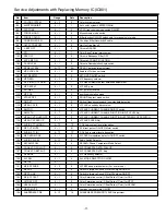
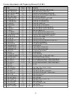
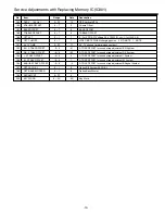
Service Adjustments with Replacing Memory IC(IC801)
No.
Item
Range
Data
Description
47
SECAM BGP SHIFT
0 ~ 3
3
Burst Gate Pulse for Position Adjustment
48
BGP SEL
0 ~ 1
0
Burst Gate Pulse Mode Select
49
PSEUDO H COIN
0 ~ 1
0
Horizontal coincidence detection by fsc counter
50
AUTO SLICE LEVEL
0 ~ 7
0
Sync separator slice level down
51
SECAM BLK LEVEL (B)
0 ~ 1
0
Sync Separator Gain Up at Vertical Sync
52
AUTO SLICE SPEED UP
0 ~ 1
0
Auto Slice Speed Switch (Normal / Up)
53
AUTO SLICE SPEED DN
0 ~ 1
0
Auto Slice Speed Switch (Normal / Down)
54
AUTO SLICE DOWN
0 ~ 1
0
Sync detect level switch during video period.
55
HV FREE
0 ~ 1
0
Horizontal and Vertical forced free-running mode switch
56
V SYNC DET TIME
0 ~ 7
0
Vertical sync detect minimum time switch
57
V SYNC DET MODE
0 ~ 1
1
Vertical sync detect mode select
58
MACRO OFF
0 ~ 1
0
Switch to improvr macrovision signal ON/OFF
59
VBLK STOP
0 ~ 1
0
Vertical blanking stop
60
EQ LATCH OFF
0 ~ 1
0
AFC1 stop timing shift
61
HBLK STOP
0 ~ 1
0
Horizontal blanking stop
62
VRAMP TEST
0 ~ 1
0
Vertical Ramp Out Test
63
V 1 WINDOW
0 ~ 1
0
Vertical sync detect mode select
64
V FREE2
0 ~ 1
0
Vertical free-running mode when horizontal coincidence is low
65
V FREE
0 ~ 1
0
Vertical forces free-running mode switch
66
FORCE V MODE
0 ~ 3
0
Vertical frequency mode switch
67 V STD DET OFF
0 ~ 1
0
Vertical frequency standard / non-standard detection
68
V STD DET2
0 ~ 1
0
Vertical frequency standard / non-standard detection
69
V FREE FREQ
0 ~ 1
0
Vertical free-running frequency
70
OSD VD DELAY
0 ~ 1
0
VD TIMING delay for OSD TIMING
71
W VBLK ON
0 ~ 1
1
Vertical blanking wide mode 16:9
72
VLOGIC STOP
0 ~ 1
0
Vertical count up logic stop
73
VBLK TEST
0 ~ 1
0
V blanking control
74
WIDE VBLK TOP
0 ~ F
0
Vertical blanking top adjustment 16:9
75
WIDE VBLK BOTTOM
0 ~ F
5
Vertical blanking bottom adjustment 16:9
76
OSD CONT CLIP LEVEL
0 ~ 3
1
Contrast control clip level of OSD mode
77
OSD CONT CLIP OFF
0 ~ 1
0
Contrast control clip switch of OSD mode
78
DRIVER (R)
0 ~ 7F
3F
R OUT amplitude adjustment by 7 bits DAC
79
BLUE BACK
0 ~ 1
0
Blue back mode ON/OFF switch
80
DRIVER (R)
0 ~ 7F
3F
B OUT amplitude adjustment by 7 bits DAC
81
WHITE BACK
0 ~ 1
0
White raster mode ON/OFF switch
82
TEST PATTERN
0 ~ 1F
0
SCREEN TEST MODE
83
PEAK ACL
0 ~ 1
0
PEAK ACL MODE ON / OFF
84
ABCL
0 ~ 1
0
ABCL ON / OFF Switch
85
ABCL GAIN
0 ~ 1
0
ABCL Gain Low / High Switch
86
DCT LEVEL
0 ~ 7
0
DC Transfer Level Control
87
DCT ON
0 ~ 1
0
DC Transfer select ON / OFF
88
COLOR CONTROL PAL
0 ~ 10
0
Color Saturation control (Offset Data of Color) for PAL
89
COLOR CONTROL NTSC
0 ~ 10
0
Color Saturation control (Offset Data of Color) for NTSC
90
COLOR CONTROL SECAM
0 ~ 10
0
Color Saturation control (Offset Data of Color) for SECAM
91
TAKE OFF
0 ~ 1
1
Chroma BPF / Take Off switch
92
C KILLER LEVEL
0 ~ 1
0
Color killer sensitivity threshold switch
SM_21-BD6V(AC7-A)Aus 11/8/07 1:14 PM Page 10
Содержание CP21VF1
Страница 35: ... 35 ...
Страница 36: ...SANYO Electric Co Ltd Nov 07 30 CPS Printed In Indonesia ...


