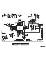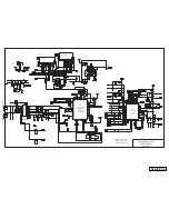
J11B5780G
K8E
1
1
2
3
4
5
6
7
8
9
10
11
12
13
14
15
16
17
18
19
20
21
22
23
24
25
26
27
28
29
30
30
A10B
30500
SP902
1
2
A10B
28900
SP901
1
2
M10B
29000
FN901
M10B
29000
FN902
J11B5780G
K11C
1
1
2
3
4
5
6
7
8
9
10
11
12
13
14
15
16
17
18
19
20
21
22
23
24
25
26
27
28
29
30
30
J11B5780G
K10C
1
1
2
3
4
5
6
7
8
9
10
11
12
13
14
15
16
17
18
19
20
21
22
23
24
25
26
27
28
29
30
30
J11B5780G
K10E
1
1
2
3
4
5
6
7
8
9
10
11
12
13
14
15
16
17
18
19
20
21
22
23
24
25
26
27
28
29
30
30
K1004
JACK-A UNIT
AV3 INPUT
K1009
PC AUDIO-IN
K1402
AV4 INPUT
K1002
ASSY,PWB,JACK-A-N2PP
1AA0B10N1010A
K1011
PC INPUT
K42G
MAIN UNIT
K69M
K7L
K69H
CN61
LCD
MODULE
CN2
CN60
CN62
CN71
CN70
CN69
1AV4U20B76300
POWER
UNIT
K16P
K16A
ASSY,PWB,SUB-N2LP
1AA0B10N1000A
SUB UNIT
K8G
K16V
K8K
K8J
KFN3
KFN2
KFN1
L
KSP9R
R
KSP9L
CN66
CN65
CN1
CN3
K1403
K8D
JACK-B UNIT
K8F
K13F
K13D
MONITOR
OUT
AV1 INPUT
ASSY,PWB,JACK-B-N2PP
1AA0B10N1010B
K8M
KEY SW UNIT
CONTROL UNIT
ASSY,PWB,KEY SW-N2PP
1AA0B10N1010E
ASSY,PWB,CONTROL-N2PP
1AA0B10N1010D
K19J
K19K
ON/OFF
POWER SW
A-SSY,PWB,POWER SW-N2PP
1AA0B10N1010F
S10B3530G
SW1901
1
2
3
4
J10EG030G
K20M
1
1
2
3
3
Z30B0120G
SC1901
1
2
1/16GJ
100C
R1919 CL1901
K20M_3
K20M_1
SC21
ASSY,PWB,FILTER N2PP
1AA0B10N1010C
3
1
3
3
(LIVE)
4
4
2
1 (NEUTRAL)
1
2
SECONDARY
PRIMARY
U20B61300
K601
1
2
3
4
S602B
275GM0.1VDA
C603
:250GM0.1XBC
:250GM0.1XBJ
:275GM0.1VB
1
2
1/2DJ220K
R603
F35B1090N
L602
1
2
3
4
Z30B
0170N
SC601
1
2
J10B2170N
KAC2
1
2
3
4
5
6
S604B
S603B
F35B1090N
L601
1
2
3
4
CL607
S601B
ENE621D14A
VA601
1
2
ENC471D14A
VA602
1
2
275GM0.1VDA
C601
:250GM0.1XBC
:250GM0.1XBJ
:275GM0.1VB
1
2
250KK680XH
C607
1
2
250KK680XH
C606
1
2
S601
S602
S604
S603
4A250VTCSL
F601
1AV4T40B58100
ASSY,PWB,MAIN-N2LP
1AA0B10N0990A
SCREW
COLOUR TELEVISION
CHASSIS
SERIES
SERVICE
REF. NO.
U
U
B
B
5
5
-
-
C
C
PRODUCT SAFETY NOTICE:
Product safety should be considered when a
component replacement is made in any area
of a receiver.
Components indicated by a mark
in this
circuit diagram show components whose
values have special significance to product
safety. It is particularly recommended that only
parts specified on the part service manual be
used for components replacement pointed out
by the mark.
CIRCUIT DIAGRAM NOTICE:
1. All resistance value are in ohms, K=1,000, M=1,000,000.
2. All resistance rated wattages are 1/6W unless otherwise noted.
3. Excepting electrolytic capacitors, all capacitance values of less than 1
are expressed in µ F and more than 1 are pF.
4. All capacitance rated voltages are 50V unless otherwise noted.
5. All inductance values are in µ H.
6. This circuit diagram covers a basic or representative chassis only. There
may be some components or partial circuit differences between the
actual chassis and the circuit diagram.
7. Parts specified with "X" are not installed in this model.
8. Parts specified with "J" are just jumper wires.
9. Expression of capacitance and resistance in circuit diagrme.
N2LVZ
TRANSISTOR, DIODE AND INTEGRATED CIRCUIT TERMINAL GUIDE
C: COLLECTOR
B: BASE
E: EMITTER
A: ANODE
K: KATHODE
B
B
C
C
E
E
C E
B
C E
B
B
C
E
A
K
K
A
A
K
FUSIBLE
RESISTOR
PARTICULAR
PARTS SYMBOL
1
1
1
N/2
N/2 + 1
N
NON POLE
ELECTRIC
CAPACITOR
POSISTER
C
E
B
CHIP
COMPONENTS
K
A
TRANSISTOR
DIODE
123
RESISTOR
12 X 103=12K
Capacitance (Example)
1000 C M 2000 D
Characteristic
Capacitance value (220pF)
Allowable error (
±
20%)
Kind (Ceramic)
Rated voltage (1,000V)
J=
±
5%
K=
±
10%
M=
±
20%
Resistance (Example)
1/2 N J 1.2
Resistance value (1.2
Ω
)
Allowable error (
±
5%)
Kind (M.carbon)
Rated wattage (1/2W)
D: Carbon
N: Metalized carbon
S: Oxied metalized
W: Wire wounding
C: Solid
T, A, U, D:
Electrolytic
C, K, B: Ceramic
F: Mylar film
M, N: Polypropylene
Z: Metalized paper
LCD-30CA1Z-00
N2LVZ-P1/8


