background image


Chapter 5 – SPI Protocol 

Revision 2.2 


SD Card Product Manual 

© 2004 SanDisk Corporation 

5-13 

12/08/04 

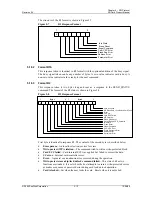
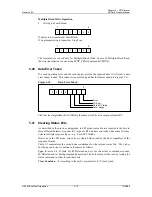
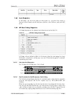
The structure of the R1 format is shown in Figure 5-7. 

Figure 5-7 

R1 Response Format 


5.18.2 Format 

R1b 

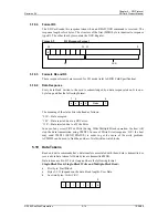
This response token is identical to R1 format with the optional addition of the busy signal. 
The busy signal token can be any number of bytes. A zero value indicates card is busy. A 
non-zero value indicates card is ready for the next command. 

5.18.3 Format 

R2 

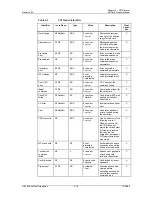
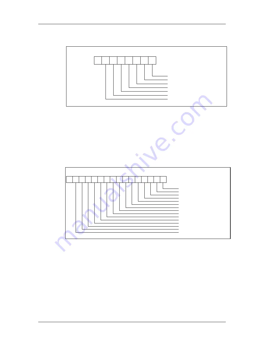
This response token is two bytes long and sent as a response to the SEND_STATUS 
command. The format of the R2 status is shown in Figure 5-8. 

Figure 5-8 

R2 Response Format 


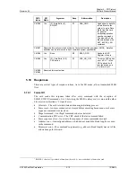
First byte is identical to response R1. The content of the second byte is described below. 

• 

Erase param

—An invalid selection, sectors for erase. 

• 

Write-protect (WP) violation

—The command tried to write a write-protected block. 

• 

Card ECC failed

—Card internal ECC was applied but failed to correct the data. 

• 

CC error

—Internal card-controller error. 

• 

Error

—A general or an unknown error occurred during the operation. 

• 

Write-protect erase-skip/lock/unlock command failed

—This status bit has two 

functions overloaded.  It is set when the host attempts to erase a write-protected sector 
or makes a sequence or password error during card lock/unlock operation. 

• 

Card is locked

—Set when the user locks the card.  Resets when it is unlocked. 

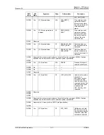
7

0

0

Idle State

Erase Reset

Illegal Command

Com CRC Error

Erase Seq Error

Address Error

Parameter Error

7

0

0

7

0

Byte 1

Byte 2

Com CRC Error

Address Error

Idle State

CC Error

WP Violation

Card is Locked

WP EraseSkip, Lock/Unlock Cmd Failed

Error

Erase Parameter

Parameter Error

Erase Reset

Illegal Command

Erase Sequence Error

Card ECC Failed

Out-of-Range, CSD_Overwrite

Содержание SDSDB-016G-A11

Страница 1: ...sk SD Card Product Manual Version 2 2 Document No 80 13 00169 November 2004 SanDisk Corporation Corporate Headquarters 140 Caspian Court Sunnyvale CA 94089 Phone 408 542 0500 Fax 408 542 0503 www sandisk com ...

Страница 2: ...ir respective companies 2004 SanDisk Corporation All rights reserved SanDisk products are covered or licensed under one or more of the following U S Patent Nos 5 070 032 5 095 344 5 168 465 5 172 338 5 198 380 5 200 959 5 268 318 5 268 870 5 272 669 5 418 752 5 602 987 Other U S and foreign patents awarded and pending Lit No 80 13 00169 Rev 2 2 119 04 Printed in U S A Revision History June 2001 Re...

Страница 3: ...e 2 2 2 6 System Reliability and Maintenance 2 2 2 7 Physical Specifications 2 3 2 8 Capacity Specifications 2 5 3 SD Card Interface Description 3 1 3 1 General Description of Pins and Registers 3 1 3 2 SD Bus Topology 3 3 3 3 SPI Bus Topology 3 5 3 4 Electrical Interface 3 6 3 5 SD Card Registers 3 11 3 6 Data Interchange Format and Card Sizes 3 23 4 SD Card Protocol Description 4 1 4 1 SD Bus Pr...

Страница 4: ... 7 5 15 Switch Function Command 5 7 5 16 High speed Mode 25MB sec interface speed 5 7 5 17 SPI Command Set 5 8 5 18 Responses 5 12 5 19 Data Tokens 5 14 5 20 Data Error Token 5 15 5 21 Clearing Status Bits 5 15 5 22 Card Registers 5 17 5 23 SPI Bus Timing Diagrams 5 17 5 24 Timing Values 5 19 5 25 SPI Electrical Interface 5 20 5 26 SPI Bus Operating Conditions 5 20 5 27 Bus Timing 5 20 Appendix A ...

Страница 5: ...as well In other words MultiMediaCard forward compatibility was kept The main difference between the SD Card and MultiMediaCard is the initialization process Matsushita Electric Company MEI Toshiba Corporation and SanDisk Corporation defined the SD Card Specification originally Currently the Secure Digital Association SDA controls the specifications The SanDisk SD Card was designed to be compatibl...

Страница 6: ...te using 4 parallel data lines Maximum data rate with up to 10 cards Correction of memory field errors Copyrights Protection mechanism Complies with highest security of SDMI standard Password protection specific models only Write Protect using mechanical switch Built in write protection features permanent and temporary Card detection Insertion Removal Application specific commands Comfortable eras...

Страница 7: ...er words systems that support the SD Card today will be able to access future SD cards built with new flash technology without having to update or change host software 1 6 Defect and Error Management SanDisk SD cards contain a sophisticated defect and error management system This system is analogous to the systems found in magnetic disk drives and in many cases offers enhancements For instance dis...

Страница 8: ...Disk SD cards have an endurance specification for each sector of 100 000 writes typical reading a logical sector is unlimited This far exceeds what is typically required in almost all SD Card applications Therefore extremely heavy use of the card in cellular phones personal communicators pagers and voice recorders will use only a fraction of the total endurance over the device s lifetime For insta...

Страница 9: ...e card to the inactive state by using the GO_INACTIVE_STATE command 1 12 3 Card Acquisition and Identification The SD Card bus is a single master SD Card host application and a multi slaves cards bus The Clock and Power lines are common to all cards on the bus During the identification process the host accesses each card separately through its own command lines The SD Card s CID Register is pre pr...

Страница 10: ...lock A unit related to block oriented read and write commands Its size is the number of bytes that are transferred when one block command is sent by the host The size of a block is either programmable or fixed information about allowed block sizes and the programmability is stored in the CSD Register The granularity of the erasable units is in general not the same as for the block oriented command...

Страница 11: ...80 1 984 000 SDSDH 512 512 1 001 216 10 240 990 976 SDSDJ 512 512 1 001 216 10 240 990 976 SDSDH 256 512 499 456 5 376 494 080 SDSDJ 256 512 499 456 5 376 494 080 SDSDJ 128 512 248 640 2 624 246 016 SDSDJ 64 512 123 232 1 376 121 856 1 All measurements are in units per card 2 The part of the card that relates to the secured copyright management and has separate DOS partitioning including sectors a...

Страница 12: ...tical to the sector size and the start address aligned to a sector boundary Multiple Block This mode is similar to the single block mode except for the host can read write multiple data blocks all have the same length that are stored or retrieved from contiguous memory addresses starting at the address specified in the command The operation is terminated with a stop transmission command Misalignme...

Страница 13: ...is set it indicates that the card is a master This feature is implemented in the card s controller firmware and not with a physical OTP cell 1 12 11 CSD Register All SD Card configuration information is stored in the CSD Register The MSB bytes of the register contain manufacturer data and the two least significant bytes contain the host controlled data the card copy write protection and the user f...

Страница 14: ...TUS can be read using ACMD13 the same as in SD mode Memory Array Partitioning Memory partitioning in SPI mode is equivalent to SD mode All read and write commands are byte addressable Read Write Operations In SPI mode single and multiple block data transfers are supported Data Transfer Rate Same as in SD mode Data Protection in the SD Card Same as in SD mode Erase Same as in SD mode Write Protecti...

Страница 15: ...g Contact Pads 4kV Human body model according to ANSI EOS ESD S5 1 1998 ESD Protection Non Contact Pad Area 8kV coupling plane discharge 15kV air discharge Human body model per IEC61000 4 2 2 3 Reliability and Durability Table 2 2 Reliability and Durability Specifications Durability 10 000 mating cycles Bending 10N Torque 0 15N m or 2 5 deg Drop Test 1 5m free fall UV Light Exposure UV 254nm 15Ws ...

Страница 16: ...ble 2 4 are under the following conditions Voltage range 2 7 V to 3 6 V Temperature 25 C to 85 C Independent of the SD Card clock frequency Table 2 4 System Performance Timing Typical Maximum Block Read Access Time 0 5 ms 100 ms Block Write Access Time 0 5 ms 250 ms CMD1 to Ready after Power up 50 ms 500 ms Sleep to Ready 1 ms 2 ms 2 6 System Reliability and Maintenance Table 2 5 Reliability and M...

Страница 17: ...ons Refer to Table 2 6 and Figure 2 1 for SD card s physical specifications and dimensions Table 2 6 SD Memory Card Physical Specification Summary Specification SD Card Weight 2 0 g maximum Length 32 mm 0 1 mm Width 24 mm 0 1 mm Thickness 2 1 mm 0 15 mm in substrate area only 2 25 mm maximum Figure 2 1 SD Memory Card Dimensions Bottom View ...

Страница 18: ...Chapter 2 Product Specifications Revision 2 2 SanDisk SD Card Product Manual 2004 SanDisk Corporation 2 4 12 08 04 Figure 2 2 SD Memory Card Dimensions ...

Страница 19: ... Figure 2 3 SD Memory Card Dimensions Top View 2 8 Capacity Specifications Table 2 7 shows the specific capacity for the various models Table 2 7 Model Capacity Summary Model No Capacity SDSDB 16 16 MB SDSDJ 32 32 MB SDSDJ 64 64 MB SDSDJ 128 128 MB SDSDJ 256 256 MB SDSDH 256 256 MB SDSDJ 512 512 MB SDSDH 512 512 MB ...

Страница 20: ...duct Specifications Revision 2 2 SanDisk SD Card Product Manual 2004 SanDisk Corporation 2 6 12 08 04 Model No Capacity SDSDJ 1024 1024 MB SDSDH 1024 1024 MB SDSDX3 1024 1024 MB SDSDJ 2048 2048 MB SDSDH 2048 2048 MB ...

Страница 21: ...SS2 S Supply voltage ground 7 DataOut O Card to host Data and Status 8 RSV 4 Reserved 9 RSV 5 Reserved 1 Type Key S power supply I input O output using push pull drivers PP I O using push pull drivers 2 The extended DAT lines DAT1 DAT3 are input on power up They start to operate as DAT lines after the SET_BUS_WIDTH command It is the responsibility of the host designer to connect external pullup re...

Страница 22: ... of a card dynamically suggested by the card and approved by the host during initialization CSD 128 Card specific data information about the card operation conditions SCR 64 SD Configuration Register information about the SD Card s special features capabilities OCR 32 Operation Condition Register The host may reset the cards by switching the power supply off and on again The card has its own power...

Страница 23: ...st and card drivers are operating in push pull mode DAT0 3 Data lines are bi directional signals Host and card drivers are operating in push pull mode CLK Clock is a host to card signal CLK operates in push pull mode VDD Power supply line for all cards VSS 1 2 Two ground lines Figure 3 2 shows the bus topology of several cards with one host in SD Bus mode Figure 3 2 SD Card System Bus Topology SD ...

Страница 24: ...edance mode RWP is used for the Write Protect Switch See Section 5 4 2 for the component values and conditions 3 2 1 Hot Insertion and Removal Hot insertion and removal are allowed inserting or removing the SD Card to or from the bus will not damage the card This also applies when the power is up The inserted card will be properly reset when CLK carries a clock frequency fpp Data transfer failures...

Страница 25: ...ol and command set The SD Card identification and addressing algorithms are replaced by the hardware CS signal A card slave is selected for every command by asserting the CS signal active low Refer to Figure 3 2 The CS signal must be continuously active for the duration of the SPI transaction command response and data The only exception is card programming time At this time the host can de assert ...

Страница 26: ...t ready for identification This bit informs the host that the card is not ready The host has to wait and continue to poll the cards each one on his turn until this bit is cleared The maximum period of power up procedure of single card shall not exceed one second Getting individual cards and the entire SD Card system out of idle state is up to the responsibility of the bus master Since the power up...

Страница 27: ... the power supply voltages The CS chip select signal timing is identical to the input signal timing see Figure 3 8 Table 3 4 Bus Operating Conditions Summary Parameter Symbol Min Max Unit Remark General Peak voltage on all lines 0 3 VDD 0 3 V All Inputs Input Leakage Current 10 10 uA All Outputs Output Leakage Current 10 10 uA Power Supply Voltage 7 Supply Voltage VDD 2 0 3 6 V CMD0 15 55 ACMD41 c...

Страница 28: ...have a variable supply voltage see Figure 3 6 Figure 3 6 Bus Signal Levels 3 4 5 Open drain Mode Bus Signal Level To meet the requirements of the JEDEC specification JESD8 1A the card input and output voltages are within the specified ranges in Table 3 6 for any VDD of the allowed voltage range Table 3 6 Input Output Voltage Parameter Symbol Min Max Unit Conditions Output high voltage VOH 0 75 VDD...

Страница 29: ...q Identification Mode 9 fOD 0 10 10 0 400 kHz CL 250 pF 21 cards Clock Low Time tWL 10 ns CL 100 pF 7 cards Clock High Time tWH 10 ns CL 100 pF 7 cards Clock Rise Time tTLH 10 ns CL 100 pF 10 cards Clock Fall Time tTHL 10 ns CL 100 pF 7 cards Clock Low Time tWL 50 ns CL 250 pF 21 cards Clock High Time tWH 50 ns CL 250 pF 21 cards Clock Rise Time tTLH 50 ns CL 250 pF 21 cards Clock Fall Time tTHL 5...

Страница 30: ...ataOut timing is illustrated in Figure 3 8 bus timing parameter values are shown in Table 3 8 Figure 3 8 Data In Out Referenced to Clock Timing high speed Table 3 8 Bus Timing Parameter Values high speed Parameter Symbol Min Max Unit Remark Clock CLK all values referred to min VIH and max VIL Clock Freq Data Transfer Mode fPP 0 50 MHz Clock Low Time tWL 7 ns Clock High Time tWH 7 ns Clock Rise Tim...

Страница 31: ...ter OCR stores the VDD voltage profile of the SanDisk SD Card The card is capable of executing the voltage recognition procedure CMD1 with any standard SD Card host using operating voltages from 2 to 3 6 V Accessing the data in the memory array however requires 2 7 to 3 6 V The OCR shows the voltage range in which the card data can be accessed The structure of the OCR Register is described in Tabl...

Страница 32: ...Five ASCII characters long Product Revision 14 BCD 8 63 56 Product Revision xx Two binary coded decimal digits Serial Number PSN Binary 32 55 24 Product Serial Number 32 bit unsigned integer Reserved 4 23 20 Manufacture Date Code MDT BCD 12 19 8 Manufacture date for ex April 2001 0x014 Manufacturing date yym offset from 2000 CRC7 checksum CRC Binary 7 7 1 CRC7 Calculated Not used always 1 1 0 0 Th...

Страница 33: ...R 119 112 1 5 msec 00100110 Data read access time 1 NSAC 8 R 111 104 0 00000000b Data read access time 2 in CLK cycles NSAC 100 Default 25MHz 0110010 TRANS_ SPEED 8 R 103 96 High speed 50MHz 01011010 Max data transfer rate CCC 12 R 95 84 All inc WP lock unlock 5F5 Card command classes READ_BL_ LEN 4 R 83 80 2G Up to 1G Ah 9h Max read data block length READ_BL_ PARTIAL 1 R 79 79 Yes 1b Partial bloc...

Страница 34: ...SIZE 7 R 38 32 128 sectors 1111111b Write protect group size WP_GRP_ ENABLE 1 R 31 31 Yes 1b Write protect group enable Reserved 2 R 30 29 0b Reserved for MMC compatibility R2W_ FACTOR 3 R 28 26 x16 0100b Write speed factor WRITE_BL_ LEN 4 R 25 22 2G Up to 1G Ah 9h Max write data block length WRITE_BL PARTIAL 1 R 21 21 No 0 Partial blocks for write allowed 5 R 20 16 00000b Reserved FILE_ FORMAT_ G...

Страница 35: ...Reserved NSAC Defines the worst case for the clock dependent factor of the data access time The unit for NSAC is 100 clock cycles Therefore the maximal value for the clock dependent part of the read access time is 25 5k clock cycles The total read access time NAC is the sum of TAAC and NSAC It has to be computed by the host for the actual clock rate The read access time should be interpreted as a ...

Страница 36: ...IAL Definition 0 Only the READ_BL_LEN block size can be used for block oriented data transfers 1 Smaller blocks can be used The minimum block size will be equal to minimum addressable unit one byte WRITE_BLK_MISALIGN Defines if the data block to be written by one command can be spread over more than one physical block of the memory device The size of the memory block is defined in WRITE_BL_LEN Tab...

Страница 37: ...ity that can be coded is 4096 512 2048 4 GB For example a 4 MB card with BLOCK_LEN 512 can be coded with C_SIZE_MULT 0 and C_SIZE 2047 VDD_R_CURR_MIN VDD_W_CURR_MIN minimum values for read and write currents at the VDD power supply are coded in Table 3 21 Table 3 21 VDD Minimum Current Consumption VDD_R_CURR MIN VDD_W_CURR MIN Code for Current Consumption VDD 2 0 0 0 5 mA 1 1 mA 2 5 mA 3 10 mA 4 2...

Страница 38: ...lue of 0 denotes 1 write block 127 denotes 128 blocks WP_GRP_SIZE contents of this register is a 5 bit binary coded value defining the number of Erase Groups see SECTOR_SIZE The actual size is computed by increasing this number by 1 A value of 0 denotes 1 erase group and a value of 127 denotes 128 erase groups WP_GRP_ENABLE A value of 0 means group write protection is not possible R2W_FACTOR defin...

Страница 39: ...ROTECT permanently protects the entire card contents against overwriting or erasing all write and erase commands for this card are permanently disabled The default value is 0 i e not permanently write protected TMP_WRITE_PROTECT temporarily protects the whole card content from being overwritten or erased all write and erase commands for this card are temporarily disabled This bit can be set and re...

Страница 40: ...h the block length was used in the command C 29 BLOCK_LEN_ ERROR E R X 0 no error 1 error The transferred block length is not allowed for this card or the number of transferred bytes does not match the block length C 28 ERASE_SEQ_ ERROR E R 0 no error 1 error An error in the sequence of erase commands occurred C 27 ERASE_ PARAM E R X 0 no error 1 error An invalid selection of write blocks for eras...

Страница 41: ...enabled 1 disabled The command has been executed without using the internal ECC A 13 ERASE_ RESET S R 0 cleared 1 reset An erase sequence was cleared before executing because an out of erase sequence command was received C 12 9 CURRENT_ STATE S X 0 idle 1 ready 2 ident 3 stby 4 tran 5 data 6 rcv 7 prg 8 dis 9 15 reserved The state of the card when receiving the command If the command execution cau...

Страница 42: ...ned by the SET_BUS_WIDTH command A 509 SECURED_MODE S R 0 not in the mode 1 secured mode Card is in Secured Mode of operation refer to the SD Security Specifications document A 508 496 Reserved 495 480 SD_CARD_TYPE S R 00xxh SD Memory Cards as defined in Physical Spec Ver 1 01 x don t care The following cards are currently defined 0000 Regular SD RD WR Card 0001 SD ROM Card In the future the 8 LSB...

Страница 43: ...d can be accessed by the host using the secured read write command after doing authentication as defined in the SD Security Specification The security protected area size is defined by SanDisk as approximately one percent of the total size of the card Tables 3 31 and 3 32 describe the user and protected areas for all SanDisk SD Cards Table 3 31 User Area DOS Image Parameters Capacity Total LBAs Nu...

Страница 44: ...2004 SanDisk Corporation 3 24 12 08 04 Capacity Total LBAs Number of Partition System Area Sectors Total Partition Sectors User Data Sectors User Data Bytes 512 MB 10 240 37 10 213 10 176 5 210 112 1 GB 20 480 37 20 421 20 384 10 436 608 2 GB 40 960 41 40 905 40 864 20 922 368 ...

Страница 45: ...is transferred via the data lines Figure 4 1 No Response and No Data Operations Card addressing is implemented using a session address that is assigned to the card during the initialization phase The basic transaction on the SD bus is the command response transaction see Figure 4 1 This type of bus transaction transfers their information directly within the command or response structure In additio...

Страница 46: ...s DAT Data from card to host Response Command Block write operation Data stop operation Response From card to host Stop command stops data transfer Command Data block CRC Busy Data block CRC Busy Multiple Block Write Operation CRC OK response and busy from card Start bit always 0 End bit always 1 Total length 48 bits 0 Content CRC Command content command and address information or parameter protec...

Страница 47: ...ed four bits at a time see Figure 4 6 Start and end bits as well as the CRC bits are transmitted for every one of the DAT lines CRC bits are calculated and checked for every DAT line individually The card sends the host the CRC status response and busy indication on DAT0 only DAT1 DAT3 during that period is don t care Figure 4 6 Data Packet Format Start bit always 0 End bit always 1 Response conte...

Страница 48: ... error conditions and timings are presented in the following sections The SanDisk SD Card has two operation modes Card Identification Mode The host will be in card identification mode after reset and while it is looking for new cards on the bus SD cards will be in this mode after reset until the SET_RCA command CMD3 is received Data Transfer Mode SD cards will enter data transfer mode when their R...

Страница 49: ...ds can use any operating voltage between VDD min and VDD max to establish communication with the host However during data transfer minimum and maximum values for VDD are defined in the Operations Condition Register OCR and may not cover the entire range Card hosts are expected to read the CSD Register and select proper VDD values or reject the card An SD Card that stores the CID and CSD data in th...

Страница 50: ...on procedure the host is not allowed to change the OCR values the SD Card will ignore changes in the OCR content If there is a real change in the operating conditions the host must reset the card stack using CMD0 and begin the initialization procedure once more However for accessing cards already in Inactive State a hard reset must be done by switching the power supply off and on GO_INACTIVE_STATE...

Страница 51: ...host issues SEND_CSD CMD9 to obtain the card specific data e g block length card storage capacity and maximum clock rate Figure 4 8 shows a block diagram of the Data Transfer Mode Figure 4 8 SD Card State Diagram Data Transfer Mode CMD7 is used to select one SD Card and place it in the Transfer State only one card can be in this state at a given time If a previously selected card is in the Transfe...

Страница 52: ...ead mode CMD56 The stop command CMD12 can abort all data write commands at any given time The write commands must be stopped prior to de selecting the card with CMD7 The write commands are block write CMD24 and CMD25 write CSD CMD27 lock unlock command CMD42 and general command in write mode CMD56 When the data transfer is complete the SD Card exits the Data Write State and moves to either the Pro...

Страница 53: ...ansmission is synchronous to the clock signal The payload for a block oriented data transfer is preserved by a CRC checksum The generator polynomial is standard CCITT format x16 x12 x5 1 Block Read The basic unit of data transfer is a block whose maximum size is defined by READ_BL_LEN in the CSD Register Smaller blocks with a starting and ending address contained entirely within one physical block...

Страница 54: ...s single write command to make faster write operation If the host uses partial blocks whose accumulated length is not block aligned and block misalignment is not allowed CSD parameter WRITE_BLK_MISALIGN is not set the card shall detect the block misalignment error and abort programming before the beginning of the first misaligned block The card shall set the ADDRESS_ERROR error bit in the status r...

Страница 55: ...e host must adhere to the following command sequence ERASE_WR_BLK_START ERASE_WR_BLK_END and ERASE CMD38 If an erase CMD38 or address setting CMD32 33 command is received out of sequence the card sets the ERASE_SEQ_ERROR bit in the Status Register and reset the entire sequence If an out of sequence command except SEND_STATUS is received the card will set the ERASE_RESET status bit in the Status Re...

Страница 56: ... a card while providing a password that will be used later for unlocking the card The password and its size are kept in 128 bit PWD and 8 bit PWD_LEN registers respectively These registers are non volatile which protects a power cycle erase Locked cards respond to and execute all commands in the basic command class class 0 ACMD41 CMD16 and lock card command class Thus the host is allowed to reset ...

Страница 57: ...the block length CMD16 given by the 8 bit card lock unlock mode the 8 bits password size in bytes and the number of bytes of the new password In case there is a password replacement the block size will consider both passwords the old and the new one are sent with the command 3 Send Card Lock Unlock command with the appropriate data block size on the data line including 16 bit CRC The data block wi...

Страница 58: ...word and to lock the card in the same sequence In such case the host performs all the required steps for setting the password as described above including the bit LOCK set while the new password command is sent If the password was previously set PWD_LEN is not 0 the card will be locked automatically after power on reset An attempt to lock a locked card or to lock a card that does not have a passwo...

Страница 59: ...rror bit will be set in the Status Register Parameter and Results of CMD42 The block length will be greater than or equal required data structure of CMD42 otherwise the result of CMD42 is undefined and the card may be in the unexpected locked state Table 4 5 clarifies the behavior of CMD42 The reserved bits in the parameter bit7 4 of CMD42 are don t care In case CMD42 requires the password it is a...

Страница 60: ... 0 0 0 0 1 0 Unlocked Exist Clear PWD_LEN PWD 0 0 0 0 1 0 Unlocked Cleared Error 12 0 1 0 0 0 1 Locked Exist Replace password card is unlocked 1 to 0 0 0 0 0 1 Unlocked Exist Replace password card is unlocked 0 0 0 0 0 1 Unlocked Cleared Set password card remains unlocked 0 0 0 0 0 0 Locked Exist Unlock card 1 to 0 0 0 0 0 0 Unlocked Exist Error 0 1 0 0 0 0 Unlocked Cleared Error 0 1 Other combina...

Страница 61: ...ite Protect and Group Write Protect are not cleared It is in need of the host clear Execute force erase and clear Temporary Write Protect and Group Write Protect 4 CMD42 Parameter 0010 and CMD42 Parameter 0110 The result is no error Card status Bit24 will be 0 Results in an error Card status Bit24 will be 1 Note The host can use both types of card without checking difference by taking account of f...

Страница 62: ...MD0 changes to 1 bit mode Note After power on in 1 bit mode if the card is locked the SD mode host shall issue CMD42 in 1 bit mode If the card is locked in 4 bit mode the SD mode host shall issue CMD42 in 4 bit mode Commands Accepted for Locked Card The locked card will accept commands listed below and return a response with setting CARD_IS_LOCKED Basic class 0 Lock card class 7 CMD16 ACMD41 All o...

Страница 63: ... as ACMD If a non ACMD is sent it the card will recognize it as a normal SD Card command and the APP_CMD bit in the Card Status stays clear If a non valid command is sent neither ACMD nor CMD it will be handled as a standard SD Card illegal command error According to SD Card protocol perspective the following ACMD numbers are reserved for the SD Card proprietary applications and may not be used by...

Страница 64: ...ll send an R1 response on the CMD line and 512 bits of status on the DAT lines The SD bus transaction considers this a standard single block read transaction and the time out value of this command is 100ms same as in read command If a CRC error occurs on the status data the host should issue a power cycle CMD6 function switching period is within eight clocks after the end bit of status data When C...

Страница 65: ...omplished by setting the argument field of the command 1 Set mode bit to 0 2 Select only one function in each function group Setting the function to 0x0 selects the default function Use appropriate values from Table 4 3 to selecting a specific function Selecting 0xF will keep the current function that was selected for the function group In response to a query the switch function status will return...

Страница 66: ...lid selection of function will be 0xF Maximum current consumption under the selected functions If one of the selected functions was strong the return value will be 0 Table 4 9 Functions Arg Slice 23 20 19 16 15 12 11 8 7 4 3 0 Group No 6 5 4 3 2 1 Function Name reserved reserved reserved reserved Command system Access mode 0x0 Default v1 01 0x1 Reserved Reserved Reserved Reserved For eC High speed...

Страница 67: ...p 6 information If a bit is set function is supported 16 479 464 Function group 5 information If a bit is set function is supported 16 463 448 Function group 4 information If a bit is set function is supported 16 447 432 Function group 3 information If a bit is set function is supported 16 431 416 Function group 2 information If a bit is set function is supported 16 415 400 Function group 1 inform...

Страница 68: ...ll terminate data transfer of CMD6 The card behavior is not guaranteed and re initialization from CMD0 is the only way to recover from undefined sate The end bit of the host command is followed on the data line with one more data bit and one end bit 2 Complete card outputs all data Figure 4 10 The card shall complete CMD6 execution and its behavior is guaranteed Complete case includes the later ti...

Страница 69: ...h speed Case 1 Check function with no error CMD6 argument 0000 0000 1111 1111 1111 1111 0000 0001 Read Data 511 496 0000 0000 0010 0000 64mA 495 400 1000 0000 0000 0001 1000 0000 0000 0001 1000 0000 0000 0001 1000 0000 0000 0001 1000 0000 0000 0011 1000 0000 0000 0011 399 376 0000 0000 0000 0000 0000 0001 375 0 Reserved All 0s Start Card version no func don t care CMD6 mode 0 func Any switch func ...

Страница 70: ...000 0000 0000 0000 0000 0001 375 0 Reserved All 0s Case 4 Switch function with error CMD6 argument 1000 0000 1111 1000 1111 0010 0000 0001 Read Data 511 496 0000 0000 0000 0000 means error 495 400 1000 0000 0000 0001 1000 0000 0000 0001 1000 0000 0000 0001 1000 0000 0000 0001 1000 0000 0000 0011 1000 0000 0000 0011 399 376 0000 1111 0000 1111 0001 0000 375 0 Reserved All 0s 4 4 11 High speed Mode1...

Страница 71: ...transfer single block read multiple block write etc of these commands When the standard command set default function 0x0 is selected the card will not recognize the commands and they will be considered illegal as defined in the SD Physical Layer Specification v1 01 When the vendor specific function 0xE is selected the commands are vendor specific They are not defined by this standard and may chang...

Страница 72: ...e the programming operation regardless of the host clock However the host must provide a clock edge for the card to turn off its busy signal Without a clock edge the card unless previously disconnected by a de select command CMD7 will permanently force the DAT line down 4 6 Cyclic Redundancy Codes The Cyclic Redundancy Check CRC is intended to protect SD Card commands responses and data transfers ...

Страница 73: ... used in single DAT line mode and in wide bus mode In wide bus mode the CRC16 is done on each line separately Figure 4 14 CRC16 Generator Checker 4 7 Error Conditions The following sections provide valuable information on error conditions 4 7 1 CRC and Illegal Commands CRC bits protect all commands If the addressed SD Card CRC check fails the card does not respond and the command is not executed T...

Страница 74: ...ommand and the start bit of the data block This number is card dependent and should be used by the host to calculate throughput and the maximal frequency for stream read Write The R2W_FACTOR field in the CSD is used to calculate the typical block program time obtained by multiplying the read access time by this factor It applies to all write erase commands e g SET CLEAR _WRITE_PROTECT PROGRAM_CSD ...

Страница 75: ...r M x x7 G x 4 8 3 Command Classes The command set of the SD Card is divided into several classes refer to Table 4 15 Each class supports a set of card functions The supported Card Command Classes CCC is coded as a parameter in the CSD Register data of each card providing the host with information on how to access the card Table 4 15 Card Command Classes Class 0 1 2 3 4 5 6 7 8 9 10 11 CMD Basic R...

Страница 76: ...D42 ACMD51 R Reserved 4 8 4 Command Description All future reserved commands and their responses must be 48 bits long Responses may not have any response Table 4 16 details the SD Card bus commands Table 4 16 SD Card Bus Command Descriptions CMD Index Type Argument Resp Abbreviation Description Basic Commands Class 0 CMD0 bc 31 0 stuff bits GO_IDLE_STATE Reset all cards to Idle State CMD1 Reserved...

Страница 77: ...rm card de selection Re send CMD3 to change its RCA number to other than 0 and use CMD7 w RCA 0 for card de selection CMD8 Reserved CMD9 ac 31 16 RCA 15 0 stuff bits R2 SEND_CSD Sends addressed card s card specific data CSD on the CMD line CMD10 ac 31 16 RCA 15 0 stuff bits R2 SEND_CID Sends addressed card s card identification CID on the CMD line CMD11 Reserved CMD12 ac 31 0 stuff bits R1b STOP_T...

Страница 78: ...rites blocks of data continuously until a STOP_TRANSMISSION command is received CMD26 Reserved for manufacturer CMD27 adtc 31 0 stuff bits R1 PROGRAM_CSD Programs the programmable bits of the CSD Write Protection Commands Class 6 CMD28 ac 31 0 data address R1b SET_WRITE_PROT If card supports this feature it sets the write protection bit of the addressed group The properties of write protection are...

Страница 79: ...the first write block to be erased CMD33 ac 31 0 data address R1 ERASE_WR_BLK_END Sets the address of the last write block of the continuous range to be erased CMD38 ac 31 0 don t care R1b ERASE Erases all previously selected write blocks CMD39 Reserved CMD40 Not valid in SD Memory Card Reserved for MultiMediaCard I O mode CMD41 Reserved I O Mode Commands Class 9 CMD39 CMD40 MMCA Optional Command ...

Страница 80: ...ends block of data to the card All the application specific commands are supported if Class 8 is allowed mandatory in SD Card CMD58 CMD59 Reserved CMD60 CMD63 Reserved for manufacturer I O Mode Commands Class 9 CMD52 CMD54 Reserved for I O mode refer to SDIO Card Specification Switch Function Commands Class 10 CMD6 adtc 31 Mode 0 0 Check function 1 Switch function 30 24 Reserved all 0 23 20 Reserv...

Страница 81: ...a bus widths are given in SCR register ACMD13 adtc 31 0 stuff bits R1 SD_STATUS Send the SD Memory Card status ACMD17 Reserved ACMD18 Reserved for SD security applications 26 ACMD19 to ACMD21 Reserved ACMD22 adtc 31 0 stuff bits R1 SEND_NUM_WR_BLOCKS Send the number of the written without errors write blocks Responds with 32bit CRC data block If WRITE_BL_PARTIAL 0 the unit of ACMD22 is always 512b...

Страница 82: ...Table 4 18 defines the SD card state transition dependent on the received command The SD Card application specific command state transitions can be found in Class 8 Table 4 18 Card State Transition Table Current Status idle ready ident stby tran data rcv prg dis ina State Change Trigger Changes to Class Independent Operation complete tran stby Class 0 CMD0 idle idle idle idle idle idle idle idle i...

Страница 83: ...ss 7 CMD42 rcv Class 8 CMD55 idle stby tran data rcv prg dis CMC56 RD WR 0 rcv CMD56 RD WR 1 data ACMD6 tran ACMD13 data ACMD22 data ACMD18 25 26 38 43 44 45 46 47 48 49 Refer to the SD Card Security Specification for an explanation of the SD Security features The SanDisk SD Card supports all the security related commands as explained in the specification ACMD41 card VDD range compatible ready ACM...

Страница 84: ...ys starts with a start bit 0 followed by the bit indicating the direction of transmission card 0 A value denoted by x in the Table 4 19 to 4 22 indicates a variable entry All responses except for the type R3 are protected by a CRC The end bit 1 terminates every response There are five types of responses supported in the SanDisk SD Card Their formats are defined as follows 1 R1 standard response re...

Страница 85: ...t transmission bit reserved CID or CSD register incl internal CRC7 end bit 4 R3 OCR Register response length 48 bits The contents of the OCR Register are sent as a response to CMD1 Table 4 21 Response R3 Bit Position 47 46 45 40 39 8 7 1 0 Width bits 1 1 6 32 7 1 Value 0 0 111111 x 111111 1 Description start bit transmission bit reserved OCR Register reserved end bit R4 and R5 responses are not su...

Страница 86: ...tors RCMD respectively RDAT Actively driven P bits are less sensitive to noise All timing values are defined in Table 4 24 4 10 1 Command and Response Card Identification and Card Operation Conditions Timing The card identification CMD2 and card operation conditions CMD1 timing are processed in the open drain mode The card response to the host command starts after exactly NID clock cycles Identifi...

Страница 87: ...e Block Read The host selects one card for data read operation by CMD7 and sets the valid block length for block oriented data transfer by CMD16 The basic bus timing for a read operation is shown in the Transfer of Single Block Read timing diagram The sequence starts with a single block read command CMD17 that specifies the start address in the argument field The response is sent on the CMD line a...

Страница 88: ... CMD line and the data transfer from the host starts NWR clock cycles after the card response was received The data is suffixed with CRC check bits to allow the card to check it for transmission errors The card sends back the CRC check result as a CRC status token on the DAT0 line In the case of transmission error the card sends a negative CRC status 101 In the case of non erroneous transmission t...

Страница 89: ... attempt to transmit the CRC status block The sequence is identical to all other stop transmission examples The end bit of the host command is followed on the data line with one more data bit end bit and two Z clock for switching the bus direction The received data block in this case is considered incomplete and will not be programmed Stop Transmission during CRC Status Transfer from the Card All ...

Страница 90: ... When a busy card which is currently in the dis state is reselected it will reinstate its busy signaling on the data line The timing diagram for this command response busy transaction is the same as given for stop tran command in the Stop Transmission Received after Last Data Block Card becomes Busy diagram above 4 13 Timing Values Table 4 24 defines all timing values Table 4 24 Timing Values Valu...

Страница 91: ...he default block length is specified in the CSD Register 512 bytes A set block length of less than 512 bytes will cause a write error The only valid write set block length is 512 bytes CMD16 is not mandatory if the default is accepted 5 2 Mode Selection The SD Card wakes up in the SD Bus mode It will enter SPI mode if the CS signal is asserted negative during the reception of the reset command CMD...

Страница 92: ...PI mode supports single block and multiple block read operations SD Card CMD17 or CMD18 Upon reception of a valid read command the card will respond with a response token followed by a data token in the length defined in a previous SET_BLOCK_LENGTH CMD16 command see Figure 5 1 Figure 5 1 Single Block Read Operation A valid data block is suffixed with a 16 bit CRC generated by the standard CCITT po...

Страница 93: ...block to be sent from the host CRC suffix and start address restrictions are identical to the read operation see Figure 5 4 The only valid block length however is 512 bytes Setting a smaller block length will cause a write error on the next write command Figure 5 4 Single Block Write Operation Command DataIn Command Response Data Error From Host to Card From Card to Host Data Error Token from Card...

Страница 94: ..._NUM_WR_BLOCKS ACMD22 in order to get the number of well written write blocks The data token s description is given in Section 5 17 Figure 5 5 Multiple Block Write Operation Resetting the CS signal while the card is busy does not terminate the programming process The card releases the dataOut line tristate and continues to program If the card is re selected before the programming has finished the ...

Страница 95: ...rable because it allows easy distinguishing between SD Memory Card and MultiMediaCard For the Thin 1 4mm SD Card CMD1 SEND_OP_COND is illegal command during the initialization that is done after power on After Power On once the card accepted valid ACMD41 it will be able to accept also CMD1 even if used after re initializing CMD0 the card It was defined in such way in order to be able to distinguis...

Страница 96: ...clock edge for the card to turn off its busy signal Without a clock edge the SD Card unless previously disconnected by de asserting the CS signal will force the dataOut line down permanently 5 10 Error Conditions The following sections provide valuable information on error conditions 5 10 1 CRC and Illegal Commands Unlike the SD Card protocol in SPI mode the card will always respond to a command T...

Страница 97: ...ite blocks WRITE_BL to be erased multiplied by the block write delay 5 11 Memory Array Partitioning See SD Card Bus Mode 5 12 Card Lock Unlock Usage of card lock and unlock commands in SPI mode is identical to SD mode In both cases the command is responded with a R1b response type After the busy signal clears the host should obtain the result of the operation by issuing a GET_STATUS command 5 13 A...

Страница 98: ...t the same set of optional command classes in both communication modes there is only one command class table in the CSD register The available command classes and the supported commands for a specific class however are different in the SD Memory Card and the SPI communication mode Note that except the classes that are not supported in SPI mode class 1 3 and 9 the mandatory required classes for the...

Страница 99: ...Command Description CMD Index SPI Mode Argument Resp Abbreviation Description CMD0 Yes None R1 GO_IDLE_STATE Resets the SD Card CMD1 Yes None R1 SEND_OP_COND Activates the card s initialization process CMD2 No CMD3 No CMD4 No CMD5 Reserved for I O mode refer to SDIO Card Specification CMD6 Yes 31 Mode 0 0 Check function 1 Switch function 30 24 Reserved all 0 23 20 Reserved for function group 6 all...

Страница 100: ... CMD19 Reserved CMD20 No CMD21 CMD23 Reserved CMD24 Yes 31 0 data address R1 WRITE_BLOCK Writes a block of the size selected by the SET_BLOCKLEN command 3 CMD25 Yes 31 0 data address R1 WRITE_MULTIPLE _BLOCK Continuously writes blocks of data until a stop transmission token is sent instead of start block CMD26 No CMD27 Yes None R1 PROGRAM_CSD Programming of the programmable bits of the CSD CMD28 Y...

Страница 101: ...te block in a continuous range to be erased CMD34 CMD37 Reserved for each command system set by switch function command CMD6 Detailed definition can be referenced in each command system specification CMD38 Yes 31 0 stuff bits R1b ERASE Erases all previously selected write blocks CMD39 No CMD40 No CMD41 Reserved CMD42 Yes 31 0 stuff bits R1 LOCK_UNLOCK Used to set re set the password or lock unlock...

Страница 102: ...acturer 5 18 Responses There are several types of response tokens As in the SD mode all are transmitted MSB first 5 18 1 Format R1 The card sends this response token after every command with the exception of SEND_STATUS commands It is 1 byte long the MSB is always set to zero and the other bits are error indications 1 signals error Idle state The card is in idle state and running initializing proc...

Страница 103: ...s for erase Write protect WP violation The command tried to write a write protected block Card ECC failed Card internal ECC was applied but failed to correct the data CC error Internal card controller error Error A general or an unknown error occurred during the operation Write protect erase skip lock unlock command failed This status bit has two functions overloaded It is set when the host attemp...

Страница 104: ...follows 010 Data accepted 101 Data rejected due to a CRC error 110 Data rejected due to a Write Error In case of any error CRC or Write during Write Multiple Block operation the host will stop the data transmission using CMD12 In case of Write Error response 110 the host may send CMD13 SEND_STATUS in order to get the cause of the write problem ACMD22 can be used to find the number of well written ...

Страница 105: ...format R2 5 21 Clearing Status Bits As described in the previous paragraphs in SPI mode status bits are reported to the host in three different formats response R1 response R2 and data error token the same bits may exist in multiple response types e g Card ECC failed However in the SD mode error bits are cleared when read by the host regardless of the response format Table 5 3 summarizes the set a...

Страница 106: ...failed C Illegal command R1 R2 E R 0 no error 1 error Command not legal for the card state C Card ECC failed R2 DataErr E X 0 success 1 failure Card internal ECC was applied but failed to correct data C CC error R2 DataErr E R X 0 no error 1 error Internal card controller error C Error R2 DataErr E R X 0 no error 1 error General or unknown error occurred during the operation C CSD overwrite R2 E R...
Страница 107: ...e host must keep the clock running for at least NCR clock cycles after the card response is received This restriction applied to command and data response tokens 5 23 1 Command and Response Host Command to Card Response Card is Ready 5 23 2 Host Command to Card Response Card is Busy The following timing diagram describes the command response transaction for commands when the card responses with th...

Страница 108: ... unknown Reading the CSD Register X H H H Z Z H H H H L L 6 byte cmd H H H H H H H H H H X X X H H Card resp L Z Z Z H L L L L L H H NCS NEC NCR CS Data In Data Out L L L H H H L L H H H H H H H H H Busy Busy H H H X X H H H H Z L NDS NEC H H H H H H H H L L L H H H 1 or 2 byte resp H H H L H H H H NCR CS Data In Data Out L H H H X X X X H H Z Z Z L H 6 byte command H H H H H H L X H H H Z Z H H H...

Страница 109: ...4 Timing Values Table 5 5 shows the timing values and definitions Table 5 5 Timing Constants Definitions Value Min Max Unit NCS 0 8 Clock cycles NCR 1 8 8 Clock cycles NRC 1 8 Clock cycles NAC 1 See Note 8 Clock cycles NWR 1 8 Clock cycles NEC 0 8 Clock cycles NDS 0 8 Clock cycles NBR 0 1 8 Clock cycles NCX 0 8 8 Clock cycles Note The maximum read access time is calculated by the host as follows N...

Страница 110: ...rporation 5 20 12 08 04 5 25 SPI Electrical Interface The SPI Mode electrical interface is identical to that of the SD Card mode 5 26 SPI Bus Operating Conditions See SD Card mode 5 27 Bus Timing See SD Card mode The timing of the CS signal is the same as any other card input ...

Страница 111: ...nformation A 1 SD Card To order SanDisk products directly from SanDisk call 408 542 0595 Part Number Block Size SDSDB 16 16 MB SDSDJ 32 32 MB SDSDJ 64 64 MB SDSDJ 128 128 MB SDSDJ 256 256 MB SDSDH 256 256 MB SDSDJ 512 512 MB SDSDH 512 512 MB SDSDJ 1024 1024 MB SDSDH 1024 1024 MB SDSDX3 1024 1024 MB SDSDJ 2048 2048 MB SDSDH 2048 2048 MB ...

Страница 112: ...nter Springs FL 32708 Tel 407 366 6490 Fax 407 366 5945 Northeastern USA Canada 620 Herndon Pkwy Suite 200 Herndon VA 22070 Tel 703 481 9828 Fax 703 437 9215 International Industrial OEM Sales Offices Europe SanDisk GmbH Karlsruher Str 2C D 30519 Hannover Germany Tel 49 511 875 9131 Fax 49 511 875 9187 Northern Europe Videroegatan 3 B S 16440 Kista Sweden Tel 46 08 75084 63 Fax 46 08 75084 26 Cent...

Страница 113: ... EXCESS OF THE PURCHASE PRICE OF THE PRODUCT ARISING OUT OF THE USE OR INABILITY TO USE SUCH PRODUCT TO THE FULL EXTENT SUCH MAY BE DISCLAIMED BY LAW SanDisk s products are not warranted to operate without failure Accordingly in any use of products in life support systems or other applications where failure could cause injury or loss of life the products should only be incorporated in systems desi...

Страница 114: ... reserves the right to market any products whether new repaired or rebuilt under different specifications and product designations if such products do not meet the original product s specifications IV RECEIVING WARRANTY SERVICE According to SanDisk s warranty procedure defective product should be returned only with prior authorization from SanDisk Corporation Please contact SanDisk s Customer Serv...

Страница 115: ...t systems or other applications where failure could cause damage injury or loss of life the products should only be incorporated in systems designed with appropriate redundancy fault tolerant or back up features SanDisk shall not be liable for any loss injury or damage caused by use of the Products in any of the following applications Special applications such as military related equipment nuclear...

Страница 116: ...ity Revision 2 2 SanDisk SD Card Product Manual 2004 SanDisk Corporation E 1 12 08 04 Appendix E Application Note E 1 Host Design Considerations NAND MMC and SD based Products SanDisk Application Note for the SanDisk SD Card follows ...

Страница 117: ...ND MMC and SD based Products Application Note Version 1 0 Document No 80 11 00160 September 30 2002 SanDisk Corporation Corporate Headquarters 140 Caspian Court Sunnyvale CA 94089 Phone 408 542 0500 Fax 408 542 0503 www sandisk com ...

Страница 118: ...se of this material All portions of SanDisk documentation are protected by copyright law and all rights are reserved This documentation may not in whole or in part be copied photocopied reproduced translated or reduced to any electronic medium or machine readable form without prior consent in writing from SanDisk Corporation SanDisk and the SanDisk logo are registered trademarks of SanDisk Corpora...

Страница 119: ...ultiMediaCard and or SD Card Timing specifications Design engineers must meet the rise fall setup hold and other SD Card and MultiMediaCard bus timing specifications If they want to support MultiMediaCards in their design the clock speed should be controllable by the host This is due to the MultiMediaCard s open drain mode the MultiMediaCard powers up in the open drain mode and cannot handle a clo...

Страница 120: ...ven the frequency of the clock you can convert the NSAC units to time and calculate the time outs in units of time The R2W_FACTOR is a read to write factor and has no units A design engineer can use the time out values derived from the CSD register to make the design compatible with all MultiMediaCards and SD cards regardless of customer brand Interface The MultiMediaCard and SD Card support multi...

Страница 121: ...to write data from the card s buffers to its internal Flash RAM and busy time to read data from the internal Flash RAM to the card s buffer Since most designs use this write and read busy time to complete other processes choosing a 1 or 4 bit bus mode can have a 4x speed effect on the time spent servicing the SD Card The example in Table 3 shows the difference between moving 512 bytes of data to a...

Страница 122: ...anning the design ensure that enough system RAM is designed in to support the multiblock capability The performance gain will always outweigh the cost of the extra RAM However if speed is not critical for example a data logger design that records only 512 bytes of data every minute Singleblock mode is more than adequate Power and Clock Control Power control should be considered when creating desig...

Страница 123: ...ding and writing to an SD Card and MultiMediaCard is generally done in 512 byte blocks however erasing often occurs in much larger blocks The NAND architecture used by SanDisk and other card vendors currently has Erase Block sizes of 32 or 64 512 byte blocks depending on card capacity In order to re write a single 512 byte block all other blocks belonging to the same Erase Block will be simultaneo...

Отзывы: