


Samsung Electronics
4-33
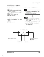
Alignment and Adjustment
b-2. Press “ENTER(CONFIRM)” button so
that the white vector moves to the center on
screen of the vectorscope.
b-3. Store the data to mode 0A2, 0A3, 0A4 and
0A5.
b-4. The OSD shows “OK!”.
6. Pre white balance (I) ; (R-Y)
1) Camera “E-E”, 3100°K gray-scale chart.
2) Video(output) jack and AF MICOM.
3) Connect vectorscope input jack to video(out-
put) jack.
4) Press the “BLC(MODE UP)/FADE(MODE
DOWN)” button so that pass through 272, 273,
274, 275 and then the OSD state is “272. XX
XX(High)””273. XX XX(Low)”.
5) Aim the camera at a 3100°K gray-scale chart
illuminated at 1500 to 2000 lx.
6) Adjust the “ P.AE(DATA UP)/DSE(DATA
DOWN)” button so that the white vector moves
to the R-Y axial on screen of the vectorscope.
Note :
Bright dot shifts after the confirm button is
pressed.
Match the white luminance
point with the
black luminance
point
Match the white luminance
point with the
black luminance
point
7. Pre white balance (II) ; (B-Y)
1) Camera “E-E”, 3100°K gray-scale chart.
2) Video(output) jack and AF MICOM.
4) Connect vectorscope input jack to video(out-
put) jack.
3) Press the “BLC (MODE UP)/FADE(MODE
DOWN)” button so that the OSD state is “274.
XX XX(High)””275. XX XX(Low)”.
5) Aim the camera at a 3100°K gray-scale chart
illuminated at 1500 to 2000 lx.
6) Adjust the “P.AE(DATA UP) /DSE(DATA
DOWN)” button so that the white vector moves
to the B-Y axial on screen of the vectorscope.
Note :
Bright dot shifts after the confirm button is
pressed.
8. R-Y Gain
1) Camera “E-E”, 3100°K color bar chart.
2) Video(output) jack and register of EEPROM.
3) Connect video(output) jack to waveform moni-
tor input jack and monitor TV jack respectively.
4) Press the “BLC(MODE UP)/FADE(MODE
DOWN)” button so that the OSD state is “280.
XX XX(High)””281. XX XX(Low)”.
5) Aim the camera at a color bar chart illuminated
at 1500 to 2000 lx.
6) Adjust the “P.AE(DATA UP)/DSE(DATA
DOWN)” button so that the red level is
NTSC : 70IRE, PAL : 500mV
7) Be sure to press the “ENTER(CONFIRM)” but-
ton to memorize setting.
Note :
Bright dot shifts after the confirm button is
pressed. (outdoor : 034, 035)
Match the white luminance
point with the
black luminance
point
70 IRE (NTSC)
500mV (PAL)
Содержание SC-L710
Страница 61: ...Samsung Electronics 4 44 Alignment and Adjustment MEMO MEMO ...
Страница 63: ...Samsung Electronics 5 2 Exploded View and Parts List 5 1 Mechanical Parts 1 600 ...
Страница 65: ...Samsung Electronics 5 4 Exploded View and Parts List 5 2 Mechanical Parts 2 ...
Страница 67: ...Samsung Electronics 5 6 Exploded View and Parts List 5 3 Mechanical Parts 3 601 ...
Страница 69: ...Samsung Electronics 5 8 Exploded View and Parts List 5 4 Ass y EVF 262 269 904 271 300 ...
Страница 71: ...Samsung Electronics 5 10 Exploded View and Parts List 5 5 Ass y Right ...
Страница 73: ...Samsung Electronics 5 12 Exploded View and Parts List 5 6 Ass y LCD ...
Страница 75: ...Samsung Electronics 5 14 Exploded View and Parts List 5 7 Ass y Left ...
Страница 77: ...Samsung Electronics 5 16 Exploded View and Parts List 5 9 Ass y Front ...
Страница 79: ...Samsung Electronics 5 18 Exploded View and Parts List 5 10 Ass y Camera Deck 116 115 ...
Страница 83: ...Samsung Electronics 5 22 Exploded View and Parts List MEMO MEMO ...
Страница 99: ...7 2 Samsung Electronics PCB Diagrams 7 1 Main PCB Component Side ...
Страница 100: ...7 3 Samsung Electronics PCB Diagrams ...
Страница 101: ...7 4 Samsung Electronics PCB Diagrams 7 2 Main PCB Conductor Side ...
Страница 102: ...7 5 Samsung Electronics PCB Diagrams ...
Страница 103: ...7 6 Samsung Electronics PCB Diagrams 7 3 Rear PCB Component Side Conductor Side ...
Страница 104: ...7 7 Samsung Electronics PCB Diagrams 7 4 EVF PCB Component Side Conductor Side ...
Страница 105: ...7 8 Samsung Electronics PCB Diagrams 7 5 Function PCB 7 6 Front PCB 7 7 LCD PCB ...
Страница 106: ...7 9 Samsung Electronics PCB Diagrams 7 8 CCD PCB Component Side Conductor Side ...
Страница 107: ...7 10 Samsung Electronics PCB Diagrams 7 9 USB PCB Component Side Conductor Side ...
Страница 108: ...8 1 Samsung Electronics 8 Wiring Diagram ...
Страница 109: ...8 2 Samsung Electronics Wiring Diagram MEMO MEMO ...
Страница 111: ...9 2 Samsung Electronics Schematic Diagrams 9 1 DC DC Converter Main ...
Страница 112: ...9 3 Samsung Electronics Schematic Diagrams 9 2 System Control Main ...
Страница 113: ...9 4 Samsung Electronics Schematic Diagrams 9 3 Audio Main ...
Страница 114: ...9 5 Samsung Electronics Schematic Diagrams 9 4 Pre Amp Main ...
Страница 115: ...9 6 Samsung Electronics Schematic Diagrams 9 5 Front ...
Страница 116: ...9 7 Samsung Electronics Schematic Diagrams 9 6 Function ...
Страница 117: ...9 8 Samsung Electronics Schematic Diagrams 9 7 EVF ...
Страница 118: ...9 9 Samsung Electronics Schematic Diagrams 9 8 LCD ...
Страница 119: ...9 10 Samsung Electronics Schematic Diagrams 9 9 CCD ...
Страница 120: ...9 11 Samsung Electronics Schematic Diagrams 9 10 CAMERA Main ...
Страница 152: ...Samsung Electronics 1 30 Operation MEMO MEMO ...


