82
- This Document can not be used without Samsung's authorization -
Ⅴ
. ADJUSTMENT
A. Purpose
Usually, although CCD sensors may have defective pixels, it is difficult to define exactly what constitutes a
defective CCD. For this reason, if the number of defective pixels is less than the permitted quantity, a CCD
sensor works by compensating for defective pixels using neighbouring pixels. To do the compensation, the
locations of the defective pixels have to be recorded.
There are two types of defective pixel. White defective pixels make an image taken in low light conditions
appear bright, whilst black defective pixels make an image taken in bright light conditions appear dark.
Only the locations of white defective pixels are recorded, since black defective pixels are rare, partly
because the results of black defective pixels are not easy to find in a JPEG image, and partly because this
reduces the checking time.
The current detection process for defect pixels has a removal function in the ARS mode for hot pixels.
B. Spec (Criteria for Checking Defects)
If the total number of defective pixels is over 256, the CCD is considered to be bad, because the maximum
number of defective pixels that the Fujitsu platform can compensate for is 256.
C. Procedures
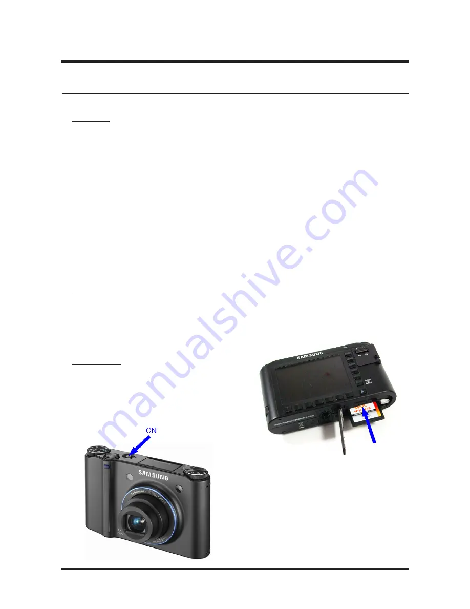
1. Copy the NV2_104.txt and adjust_t files
onto the root directory of the SD card and
install the card into the camera.
2. Turn on the camera and the Adjustment mode will
be selected automatically.
12. Defective CCD Pixel Test
Содержание NV24HD
Страница 1: ......
Страница 87: ... This Document can not be used without Samsung s authorization Ⅵ BLOCK DIAGRAM 87 ...
Страница 89: ...89 This Document can not be used without Samsung s authorization Ⅶ PATTERN DIAGRAM 2 MAIN_BOTTOM ...
Страница 90: ...90 This Document can not be used without Samsung s authorization Ⅷ CIRCUIT DIAGRAM 1 MAIN_SUB CONNECTOR ...
Страница 91: ...91 This Document can not be used without Samsung s authorization Ⅷ CIRCUIT DIAGRAM 2 MAIN_PRE_LAYOUT ...
Страница 92: ...92 This Document can not be used without Samsung s authorization Ⅷ CIRCUIT DIAGRAM 3 MAIN_AFE BLOCK ...
Страница 93: ...93 This Document can not be used without Samsung s authorization Ⅷ CIRCUIT DIAGRAM 4 MAIN_MEMORY ...
Страница 94: ...94 This Document can not be used without Samsung s authorization Ⅷ CIRCUIT DIAGRAM 5 MAIN_MICOM ...
Страница 95: ...95 This Document can not be used without Samsung s authorization Ⅷ CIRCUIT DIAGRAM 6 MAIN_MOTOR ...
Страница 96: ...96 This Document can not be used without Samsung s authorization Ⅷ CIRCUIT DIAGRAM 7 MAIN_EXP I F HDMI 30P ...
Страница 97: ...97 This Document can not be used without Samsung s authorization Ⅷ CIRCUIT DIAGRAM 8 MAIN_POWER IC ...
Страница 98: ...98 This Document can not be used without Samsung s authorization Ⅷ CIRCUIT DIAGRAM 9 MAIN_AM O LED LCD ...
Страница 100: ...100 This Document can not be used without Samsung s authorization Ⅷ CIRCUIT DIAGRAM 11 MAIN_CARD B D COM ...


