1. Precautions
Follow these safety, ESD, and servicing precautions to prevent personal injury and equipment damage.
1-1 Safety Precautions
1. Be sure that all built-in protective devices are in
place. Restore any missing protective shields.
2. Make sure there are no cabinet openings through
which people- particularly children- might insert
fingers or objects and contact dangerous voltages.
3. When re-installing chassis and assemblies, be
sure to restore all protective devices, including
control knobs and compartment covers.
4. Design Alteration Warning:
Never alter or add to the mechanical or electrical
design of this equipment, such as auxiliary
connectors, etc. Such alterations and
modifications will void the manufacturer’s
warranty.
5. Components, parts, and wiring that appear to
have overheated or are otherwise damaged
should be replaced with parts which meet the
original specifications. Always determine the
cause of damage or overheating, and correct any
potential hazards.
6. Observe the original lead dress, especially near
sharp edges, AC, and high voltage power
supplies. Always inspect for pinched, out-of-
place, or frayed wiring. Do not change the
spacing between components and the printed
circuit board.
7. Product Safety Notice:
Some electrical and mechanical parts have special
safety-related characteristics which might not be
obvious from visual inspection. These safety
features and the protection they provide could be
lost if a replacement component differs from the
original. This holds true, even though the
replacement may be rated for higher voltage,
wattage, etc.
Components critical for safety are indicated in
the parts list with symbols . Use only
replacement components that have the same
ratings, especially for flame resistance and
dielectric specifications. A replacement part that
does not have the same safety characteristics as
the original may create shock, fire, or other safety
hazards.
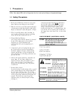
LASER STATEMENT (LASERTURVALLISUUS)
WARNING : NEVER OPERATE AND SERVICE THE PRINTER
WITH THE PROTECTIVE COVER REMOVED
FROM LASER/SCANNER ASSEMBLY. THE
REFLECTIVE BEAM, ALTHOUGH INVISIBLE, CAN
DAMAGE YOUR EYES.
Class 1 laser product
Luokan 1 laserlaite
Klass 1 laser apparat
Allonpituus 770-795nm
Teho 0.3mW±0.03mW
Samsung Electronics
1-1
CAUTION
VORSICHT
ATTENTION
ATTENZIONE
PRECAUCION
CAUTION :
Avoid exposure to invisible laser radiation when the
development unit is not installed.
INVISIBLE LASER RADIATION WHEN
THIS COVER OPEN. DO NOT OPEN
THIS COVER.
UNSICHTBARE LASERSTRAHLUNG,
WENN ABDECKUNG GEOFFNET.
NIGHT DEM STRAHL AUSSETZEN.
REYONNEMENT LASER INVISIBLE EN CAS
D’OUVERTURE. EXPOSITION DANGERUSE AU
FAISCEAU.
RADIAZIONE LASER INVISIBLE IN CASO DI
APERTURA. EVITARE L’ESPOSIZONE LA FASCIO.
REDIACION LASER INVISIBLE CUANDO SE
ABRE. EVITAR EXPONERSE AL RAYO.
Содержание Msys 6750
Страница 2: ...ELECTRONICS Samsung Electronics Co Ltd December 1999 Printed in Korea VERSION NO 2 00 P N JC81 00285A ...
Страница 10: ...2 6 Samsung Electronics Specification Memo ...
Страница 58: ...4 28 Samsung Electronics Maintenance Troubleshooting MEMO ...
Страница 81: ...5 22 Samsung Electronics Exploded Views and Parts Lists MEMO ...
Страница 95: ...MEMO Samsung Electronics 8 2 ...
Страница 96: ...PCB Diagrams Samsung Electronics 9 1 9 1 Main PCB Diagram Top 9 PCB Diagrams ...
Страница 97: ...PCB Diagrams Samsung Electronics 9 2 9 2 Main PCB Diagram Bottom ...
Страница 98: ...PCB Diagrams Samsung Electronics 9 3 9 3 LIU PCB Diagram Top 9 4 LIU PCB Diagram Bottom ...
Страница 99: ...PCB Diagrams Samsung Electronics 9 4 9 5 Engine PCB Diagram Top ...
Страница 100: ...PCB Diagrams Samsung Electronics 9 5 Engine PCB Diagram Top ...
Страница 101: ...PCB Diagrams Samsung Electronics 9 6 9 6 Engine PCB Diagram Bottom ...
Страница 102: ...PCB Diagrams Samsung Electronics 9 7 Engine PCB Diagram Bottom ...
Страница 103: ...PCB Diagrams Samsung Electronics 9 8 9 7 OPE PCB Diagram ...
Страница 104: ...PCB Diagrams Samsung Electronics 9 9 OPE PCB Diagram ...
Страница 105: ...PCB Diagrams Samsung Electronics 9 10 MEMO ...
Страница 106: ...Connection diagram Samsung Electronics 8 1 8 Connection diagram ...
Страница 107: ...MEMO Samsung Electronics 8 2 ...
Страница 110: ...Main Circuit Diagram 3 5 Samsung Electronics 10 3 Schematic Diagrams ...
Страница 111: ...Schematic Diagrams 10 4 Samsung Electronics Main Circuit Diagram 4 5 ...
Страница 113: ...Schematic Diagrams 10 6 Samsung Electronics 10 2 Engine Circuit Diagram 1 4 ...
Страница 114: ...Engine Circuit Diagram 2 4 Samsung Electronics 10 7 Schematic Diagrams ...
Страница 115: ...Schematic Diagrams 10 8 Samsung Electronics Engine Circuit Diagram 3 4 ...
Страница 116: ...Engine Circuit Diagram 4 4 Samsung Electronics 10 9 Schematic Diagrams ...
Страница 117: ...Schematic Diagrams 10 10 Samsung Electronics 10 3 LIU Circuit Diagram ...
Страница 118: ...10 4 OPE Circuit Diagram Samsung Electronics 10 11 Schematic Diagrams D6 D5 D4 D3 D2 D1 D0 D6 D5 D0 D1 D2 D3 D4 ...


