


3 Alignments and Adjustments
3-10
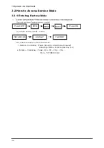
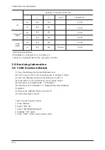
3-6 Servicing Information
3-6-1 USB Download Method
(1) Copy the Software file into the USB flash driver.
(2) Turn on your LCD TV and check the source is 'Analog TV Mode'.
(3) Insert the USB flash driver into the USB Jack of LCD TV.
(4) Press 'Mute'+'7'+'8'+'9'+'Exit' keys of your remote control.
(5) The banner osd "Updating SW..." is displayed.
(6) The banner osd "Completed..." is displayed when the updating is
completed.
(7) Remove the USB flash driver from LCD TV.
(8) Check the program version.
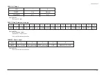
* How to check Program Version
1. Press " MENU "
2. Select " SET UP "
3. Select " INFORMATION HELP "
4. Highlight " ON " option
5. Press " INFO " button on the remote control
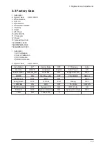
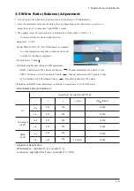
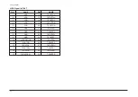
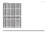
AV
L/L
H/L
H/L
L/L
H/L
L/L
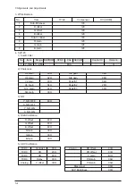
T(K) + MPCD
Y (cd/m
2
)
-
-
-
-
-
13.2cd/
m
2
y
283
Adjustment Coordinate (LE46F71B)
x
268
268
283
283
283
283
283
268
268
268
268
12,000
12,000
12,000
12,000
12,000
12,000
Component
(720P)
HDMI
(720P)
- Adjustment Specification
White Balance : High light (
2), Low light (
3)
Luminance : High light (Don't care), Low light (
0.2 Ft/L)
Содержание LA40F71BX
Страница 3: ...Contents...
Страница 4: ...Contents...
Страница 25: ...11 Disassembly and Reassembly 11 10 Memo...
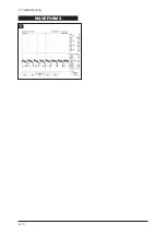
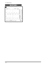
Страница 29: ...4 Troubleshooting 4 4 WAVEFORMS 1...
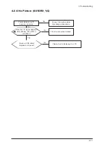
Страница 31: ...4 Troubleshooting 4 6 2...
Страница 33: ...4 Troubleshooting 4 8 WAVEFORMS 4 3...
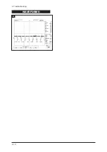
Страница 35: ...4 Troubleshooting 4 10 WAVEFORMS 5...
Страница 37: ...4 Troubleshooting 4 12 6 WAVEFORMS...
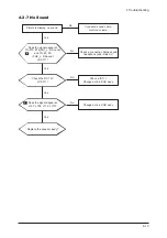
Страница 39: ...4 Troubleshooting 4 14 WAVEFORMS 7...
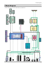
Страница 50: ...7 Block Diagrams 7 1 7 Block Diagram This Document can not be used without Samsung s authorization...
Страница 51: ...7 Block Diagrams 7 2 Memo...
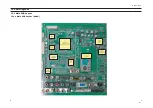
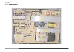
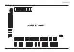
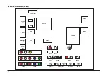
Страница 52: ...12 PCB Diagram 12 1 12 PCB Diagram 12 1 Main PCB Layout 12 1 1 Main PCB Layout 40 46...
Страница 53: ...12 PCB Diagram 12 2 12 1 2 Main PCB Layout 52...
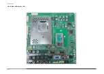
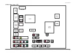
Страница 54: ...12 PCB Diagram 12 3 12 2 IP Board Diagram 40...
Страница 55: ...12 PCB Diagram 12 4 12 3 IP BOARD Diagram 46...
Страница 56: ...8 1 8 Wiring Diagrams 8 Wiring Diagram 8 1 Wiring Diagram...
Страница 69: ...8 Wiring Diagrams 8 14 Memo...
Страница 146: ...13 Circuit Descriptions 13 3 13 2 Main Block...
Страница 147: ...13 Circuit Descriptions 13 4 13 3 IP Board...
Страница 153: ...Memo 10 Operating Instructions and Installation 10 6...
Страница 161: ...14 Reference Infomation 14 8 14 3 2 Supported Modes 1...
Страница 162: ...14 Reference Infomation 14 9 14 3 3 Supported Modes 2...
Страница 163: ...14 Reference Infomation 14 10 14 3 4 Supported Modes 3...
Страница 173: ...Memo 1 Precautions 1 4...
Страница 175: ...9 Schematic Diagrams 9 2 9 2 Input Output Schematic Diagram...
Страница 176: ...9 Schematic Diagrams 9 3 9 3 Input Output Schematic Diagram...
Страница 177: ...9 Schematic Diagrams 9 4 9 4 Micom Schematic Diagram...
Страница 178: ...9 Schematic Diagrams 9 5 9 5 SVP LX Schematic Diagram 9 5 1 SVP LX Schematic Diagram 40 46...
Страница 179: ...9 Schematic Diagrams 9 6 9 5 2 SVP LX Schematic Diagram 52...
Страница 180: ...9 Schematic Diagrams 9 7 9 6 Application Schematic Diagram...
Страница 181: ...9 Schematic Diagrams 9 8 9 7 FRCH 100Hz LVDS Schematic Diagram...


