


3 Alignments and Adjustments
3-9
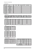
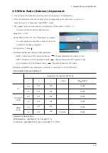
1.
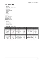
You can adjust the white ratio in factory mode (1:Calibration, 3:White-Balance).
2. Since the adjustment value and the data value vary depending on the input source, you have to
adjust these in AV, Component 1 and HDMI 1 modes.
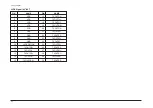
3. The optimal values for each mode are configured by default. (Refer to Table 1, 2.)
It varies with Panel's size and Specification.
- Equipment : CS-210
- Pattern: MIK K-7256 #92 "Flat W/B Pattern" as standard
- Use other equipment only after comparing the result
with that of the Master equipment.
- Set Aging time : 60min
- Calibration and Manual setting for WB adjustment.
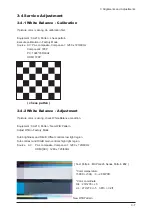
HDMI : Calibration at #24 Chessboard Pattern Manual adjustment #92 pattern (720p)
COMP: Calibration at #24 Chessboard Pattern Manual adjustment at #92 pattern (720p)
AV Calibration at #24 Chessboard Pattern Manual adjustment at #92 pattern
- If finishing in HDMI mode, adjustment coordinate is almost same in AV/COMP mode.
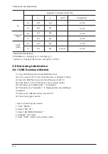
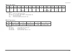
278
278
278
278
278
AV
L/L
H/L
H/L
L/L
H/L
L/L
T(K) + MPCD
Y (cd/m
2
)
-
-
-
-
-
13.2cd/
m
2
y
278
Adjustment Coordinate (LE40F71B)
x
272
272
272
272
272
272
12,000
12,000
12,000
12,000
12,000
12,000
Component
(720P)
HDMI
(720P)
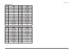
- White Balance Manual Adjustment
- Adjustment Specification
White Balance : High light (
2), Low light (
3)
Luminance : High light (Don't care), Low light (
0.2 Ft/L)
3-5 White Ratio (Balance) Adjustment
Содержание LA40F71BX
Страница 3: ...Contents...
Страница 4: ...Contents...
Страница 25: ...11 Disassembly and Reassembly 11 10 Memo...
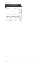
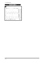
Страница 29: ...4 Troubleshooting 4 4 WAVEFORMS 1...
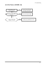
Страница 31: ...4 Troubleshooting 4 6 2...
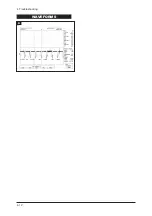
Страница 33: ...4 Troubleshooting 4 8 WAVEFORMS 4 3...
Страница 35: ...4 Troubleshooting 4 10 WAVEFORMS 5...
Страница 37: ...4 Troubleshooting 4 12 6 WAVEFORMS...
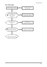
Страница 39: ...4 Troubleshooting 4 14 WAVEFORMS 7...
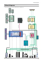
Страница 50: ...7 Block Diagrams 7 1 7 Block Diagram This Document can not be used without Samsung s authorization...
Страница 51: ...7 Block Diagrams 7 2 Memo...
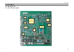
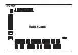
Страница 52: ...12 PCB Diagram 12 1 12 PCB Diagram 12 1 Main PCB Layout 12 1 1 Main PCB Layout 40 46...
Страница 53: ...12 PCB Diagram 12 2 12 1 2 Main PCB Layout 52...
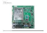
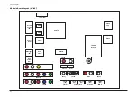
Страница 54: ...12 PCB Diagram 12 3 12 2 IP Board Diagram 40...
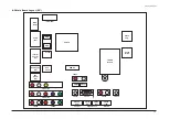
Страница 55: ...12 PCB Diagram 12 4 12 3 IP BOARD Diagram 46...
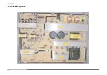
Страница 56: ...8 1 8 Wiring Diagrams 8 Wiring Diagram 8 1 Wiring Diagram...
Страница 69: ...8 Wiring Diagrams 8 14 Memo...
Страница 146: ...13 Circuit Descriptions 13 3 13 2 Main Block...
Страница 147: ...13 Circuit Descriptions 13 4 13 3 IP Board...
Страница 153: ...Memo 10 Operating Instructions and Installation 10 6...
Страница 161: ...14 Reference Infomation 14 8 14 3 2 Supported Modes 1...
Страница 162: ...14 Reference Infomation 14 9 14 3 3 Supported Modes 2...
Страница 163: ...14 Reference Infomation 14 10 14 3 4 Supported Modes 3...
Страница 173: ...Memo 1 Precautions 1 4...
Страница 175: ...9 Schematic Diagrams 9 2 9 2 Input Output Schematic Diagram...
Страница 176: ...9 Schematic Diagrams 9 3 9 3 Input Output Schematic Diagram...
Страница 177: ...9 Schematic Diagrams 9 4 9 4 Micom Schematic Diagram...
Страница 178: ...9 Schematic Diagrams 9 5 9 5 SVP LX Schematic Diagram 9 5 1 SVP LX Schematic Diagram 40 46...
Страница 179: ...9 Schematic Diagrams 9 6 9 5 2 SVP LX Schematic Diagram 52...
Страница 180: ...9 Schematic Diagrams 9 7 9 6 Application Schematic Diagram...
Страница 181: ...9 Schematic Diagrams 9 8 9 7 FRCH 100Hz LVDS Schematic Diagram...


