background image

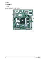
13-2-1 Main SMPS

1. Summary
This is a service manual about the explanation of basic operation in power circuit (1H309W) for 50" PDP.

2. Input Part
This switching mode power supply (SMPS) has the input voltage range of 90 ~ 264[Vac].
Thus, at 90[Vac] input condition or any voltage level in a spec, the power board must operate even if the ac source is cut off and
re-input ON.

3. Output Part
This power circuit has the 10 outputs. In steady state, the specification about the output's voltage and current is the same as
following Table 1.

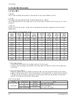
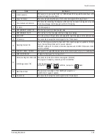
Table 1. PDP SMPS's output specifications (for 50")

Over Voltage Protectionl

This power circuit has the function of over voltage protection (O.V.P) in all outputs.
In condition of any over voltage in each output ports, the power supply is shut-down by O.V.P function for the protection of 
part's damage.

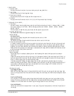
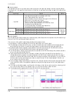
Short / Over Current Protection

Because any output ports have small impedance (smaller than 300m ohm) at the output short condition, power circuit was 
designed to have the function of short / over current protection (O.C.P) in all outputs. Thus, in condition of any over current in 
each output ports, the power supply is shut-down by O.C.P function for the protection of part's damage. The specification 
about the O.C.P in each port is the same as following Table 2.

Table 2. OCP specification

Output

Circuit

Nominal

Voltage

[V]

Voltage

Adjustment

[V]

Total

Regulation

Nominal

Load

[A]

Load

Variation

[A]

Peak

Current

[A]

Ripple

Noise

[mV p-p]

Vs

210

190 - 220

±

2%

1.7

0.1 - 2.5

10.0

800

Va

70

60 - 80

±

2%

0.7

0.1 - 3.0

4.5

500

D5.3V

5.3

----------

±

5%

3.5

0.1 - 5.0

6.0

50

A6.5V

6.5

----------

±

5%

1.5

0.01 - 3.0

4.0

50

FAN_8V

8

----------

±

5%

-

0.01 - 0.2

0.5

120

Vg

15

----------

±

5%

0.5

0.01 - 1.0

1.5

120

12V

12

----------

±

5%

1.3

0.01 - 1.5

3.0

120

Vamp

18

----------

±

10%

0.1

0.01 - 2.5

3.0

180

Vt

33

----------

±

5%

5m

1m - 6m

7m

300

STBY

5.0

----------

±

5%

0.5

0.01 - 1.0

1.5

50

Protection

Output Circuit

Trip point

Notes

Over Current

Vs

3.0 - 6.0A

Shut down by Under Voltage

Va

3.5A or more

Short Circuit Protection
Shut down by Under Voltage

Output except Vs&Va

----------

Circuit Description

13-2

Samsung Electronics

13-2 Partial Block Description

Содержание HPS5033 - 50" Plasma TV

Страница 1: ...033X XAA PLASMA DISPLAY TV FEATURES NTSC ATSC Tuner Built In 13 Bit Processing 549 Billion Colors Split Screen Picture In Picture Samsung DNIe Digital Natural Image engine SRS TruSurround XT 2 HDMI Input Energy Saving SAMSUNG EPG System SERVICE Manual HP S5033 ...

Страница 2: ... Manual is a property of Samsung Electronics Co Ltd Any unauthorized use of Manual can be punished under applicable International and or domestic law Samsung Electronics Co Ltd Jun 2006 Printed in Korea AA82 03790A ...

Страница 3: ...How to Access Service Mode 3 2 3 3 Factory Data 3 3 3 4 Service Adjustment 3 21 3 5 Software Upgrade 3 25 3 6 Replacements Calibration 3 26 Chapter 4 Exploded View Part List 4 1 HPS5033X XAA 4 1 Chapter 5 Electrical Part List 5 1 HPS5033X XAA Service Item 5 1 Chapter 6 Troubleshooting 6 1 First Checklist for Troubleshooting 6 1 6 2 Checkpoints by Error Mode 6 2 6 3 Troubleshooting Procedures by AS...

Страница 4: ...10 7 10 8 PC HDMI INPUT 10 8 10 9 VIDEO DECODER SCALER SVP PX 10 9 10 10 SVP PX DDR MEMORY 10 10 10 11 SVP PX POWER BLOCK 10 11 10 12 LBE PWM CONTROL PANEL I F 10 12 10 13 LAKE I2C GPIO USB UART INT 10 13 10 14 LAKE I2S IN OUT TS IN YCbCr OUT 10 14 10 15 LAKE DDR MEMORY 10 15 10 16 LAKE STATIC MEMORY DEBUG 10 16 10 17 LAKE POWER BLOCK 10 17 10 18 MPEG ENCODER SAA6752 10 18 10 19 TC90103AFG 10 19 C...

Страница 5: ...3 Circuit Description 13 1 Power ON OFF Signal Timing Sequence 13 1 13 2 Partial Block Description 13 2 Chapter 14 Reference Information 14 1 Other issues related to other products 14 1 14 2 Technical Terms 14 3 ...

Страница 6: ...out insulated transformers the product can only be repaired safely when the chassis is connected to the earthed end of the AC power source To make sure the AC power cord is properly connected follow the instructions below Use the voltmeter to measure the voltage between the chassis and the earthed ground If the measurement is over 1 0V unplug the AC power cord and change the polarity before re ins...

Страница 7: ...eplaced with another irregular one the safety or protective features will be lost even if the new one has a higher voltage or more watts Critical safety parts should be bracketed with Use only regular parts for replacements in particular flame resistance and dielectric strength specifications Irregular parts or materials may cause electric shock or fire Precaution 1 2 Samsung Electronics ...

Страница 8: ...sistance between the blade of the AC plug and that of the conductive material should be more than 1 7 Any B interlock should not be damaged If the metal heat sink is not properly installed no connection to the AC power should be made 8 Make sure the grounding lead of the tester is connected to the chassis ground before connecting to the positive lead The ground lead of the tester should be removed...

Страница 9: ... for soldering purposes 6 Use only anti static solder removal devices Most solder removal devices do not support an anti static feature A solder removal device without an anti static feature can store enough static electricity to cause damage to the ESD 7 Do not remove the ESD from the protective box until the replacement is ready Most ESD replacements are covered with lead which will cause a shor...

Страница 10: ...ositioning the product Also check the antenna cable or the external connectors if they are fully unplugged Damage to the cord may cause fire or electric shock 6 Keep the antenna far away from any high voltage cables and install it firmly Contact with the high voltage cable or the antenna falling over may cause fire or electric shock 7 When connecting the RF antenna check for a DTV receiving system...

Страница 11: ...1 6 Samsung Electronics MEMO ...

Страница 12: ...nt PC Lake SDP54 Sound Speaker 10W 10W SRS TruSurround XT Dolby Digital STV8258 STA323W Optical Coaxial Output Cabinet E7 Design New Cabinet Chip Description DNVS303HH261A Tuner ATSC NTSC VSB NIM Tuner SVP PX Component CVBS Y C HDMI PC input Video signal processor SDP54 The DNIe IC for visual quality improvement LBE STV8258 Sound Processing IC STA323W Sound AMP IC S5H2111X01 MPEG Decoder IC Lake 3...

Страница 13: ... 50 inches ANTENNA input ANT 1 AIR IN ANT 2 CABLE IN 75Ω unbalanced VIDEO input AV1 AV2 S VIDEO1 S VIDEO2 COMPONENT1 480i 480p 720p 1080i COMPONENT2 480i 480p 720p 1080i PC HDMI1 DVI Compatible 480p 720p 1080i HDMI2 480p 720p 1080i AUDIO input AV1 AV2 S VIDEO1 S VIDEO2 COMPONENT1 480i 480p 720p 1080i COMPONENT2 480i 480p 720p 1080i PC DVI AV Output AUDIO L R Speaker Output 10W 10W 8Ω Audio Output ...

Страница 14: ...Ie LBE Still picture Noise reduction Comb Filter 3D comb filter PIP Large Double1 Double2 Picture Size 16 9 Zoom1 Zoom2 4 3 AV S Video Component 480i 480p 16 9 4 3 Component 720p 1080i PC HDMI Sound System Stereo Dolby Digital TruSurround XT Output 10W 10W Speaker Built in Optical Coaxial Sound Output Dolby Digital PCM DTV PCM HDMI Feature Component Interface 480i 480p 720p 1080i Y Pb Pr Digital I...

Страница 15: ...00 37 500 N N 800 X 600 56 250 35 156 N P N P 60 317 37 879 P P 70 000 43 75 N P N P 72 188 48 077 P P 75 000 46 875 P P 1024 X 768 60 004 48 363 N N 70 069 56 476 N N 72 000 57 672 N P N P 75 029 60 023 P P 1280 X 720 59 855 44 772 P N 1360 X 768 60 015 47 712 P P The interlace mode is not supported The TV operates abnormally if a non standard video format is selected The table above conforms to ...

Страница 16: ... Stand Picture Brightness 1 000 Cd m2 1 000 Cd m2 1 300 Cd m2 Contrast Ratio 10 000 1 3 000 1 10 000 1 Picture Enhacer DNIe LBE DNIe 2 DNIe Lite Comb Filter Audio Equalizer 5 Band 5 Band 5 Band Auto Volume Control Surround Sound SRS TruSurround XT Dolby Digital SRS TruSurround XT SRS TruSurround XT Dolby Digital Speaker Output 10W 10W 15W 15W 15W 15W Features PIP Double Window Caption Still Image ...

Страница 17: ...BN68 00872A AA68 03870A AA68 03242F Remote Control AAA Batteries BN59 00511A 4301 000103 Power Cord 3903 000144 Ferrite Core for Power Cord 3301 001110 Ferrite Core for Side AV 3301 001305 Accessories that can be purchased additionally S VIDEO Cable BN39 00149A Internal shopping mall HDMI Cable BN39 00641A HDMI DVI cable BN39 00643A Component Cables RCA BN39 00279A PC Cable BN39 00115A PC Audio Ca...

Страница 18: ...ent Adjustment 3 1 Service Instruction Before Performing After Sales Services 1 Check if the measurement and test equipment is working properly 2 Secure sufficient work space for disassembling the product 3 Prepare a soft pad for disassembling the product ...

Страница 19: ... Key Select an item Volume Key Adjust the value up or down MENU Key Save the changes to the EEPROM and return to the higher level mode Using the Numeric 0 9 keys you can select a channel Using the SOURCE key you can switch AV modes 5 Initial SERVICE MODE DISPLAY State The version of the firmware displayed at the bottom of the screen may differ and the firmware is subject to change for the improvem...

Страница 20: ...K ANYNET Gamma PDP OFF PDP ACR PDP ACR OFF ACR HSCB PDP HSCB BASE HSCB Panel Display Time XX Hr Mute Time RF 2 CH Memory SAMEX None Suwon SAMEX ITEM Range RF AV S Video Component PC HDMI DTV Sub Brightness LBE 0 255 128 128 128 128 R Offset 0 1023 512 512 512 512 G Offset 0 1023 512 512 512 512 B offset 0 1023 512 511 512 512 512 512 Sub Contrast LBE 0 255 128 128 128 128 R Gain 0 1023 512 512 512...

Страница 21: ...tem 42SD Movie Skin Value 1 RF x 1560 y 1630 2 AV x 1560 y 1630 3 480i x 1550 y 1620 4 480p x 1580 y 1620 5 720p 1080i x 1690 y 1630 42HD Movie Mode Option Item 1 RF x 1490 y 1655 2 AV x 1500 y 1700 3 480i x 1570 y 1655 4 480p x 1570 y 1655 5 720p 1080i The same as Dynamic 50HD Movie Mode Option Item 1 RF Video x 1470 y 1660 2 Comp 480i x 1580 y 1640 3 Comp 480p x 1680 y 1700 4 Comp 720p The same ...

Страница 22: ...n 29 30 31 W1_ROffset 2 3 2 W1_BOffset 2 1 2 W2_RGain 27 27 22 W2_BGain 50 48 43 W2_ROffset 1 3 1 W2_BOffset 1 2 2 NOR_RGain 2 19 6 NOR_BGain 21 12 10 NOR_ROffset 3 6 1 NOR_BOffset 0 0 4 C2_RGain 20 2 7 C2_BGain 14 16 21 C2_ROffset 9 3 0 C2_BOffset 1 0 5 Movie Contrast 55 55 55 55 55 55 55 55 55 55 55 55 Movie Bright 55 55 55 55 55 55 55 55 55 55 55 55 Movie Color 20 20 20 20 20 20 20 20 20 20 20 ...

Страница 23: ...1_BGain 39 28 27 W1_ROffset 1 1 0 W1_BOffset 5 0 0 W2_RGain 27 10 23 W2_BGain 50 45 40 W2_ROffset 0 1 4 W2_BOffset 3 1 0 NOR_RGain 9 3 6 NOR_BGain 15 10 16 NOR_ROffset 1 1 1 NOR_BOffset 1 1 2 C2_RGain 5 4 9 C2_BGain 9 5 14 C2_ROffset 2 2 2 C2_BOffset 0 3 1 Movie Contrast 55 55 55 55 55 55 55 55 55 55 55 55 Movie Bright 55 55 55 55 55 55 55 55 55 55 55 55 Movie Color 20 20 20 20 20 20 20 20 20 20 2...

Страница 24: ...1_BGain 40 29 33 W1_ROffset 0 0 2 W1_BOffset 7 0 2 W2_RGain 26 13 20 W2_BGain 48 46 46 W2_ROffset 1 1 1 W2_BOffset 3 1 1 NOR_RGain 10 4 4 NOR_BGain 16 12 18 NOR_ROffset 1 1 3 NOR_BOffset 1 1 2 C2_RGain 5 2 12 C2_BGain 12 5 5 C2_ROffset 2 2 4 C2_BOffset 1 1 4 Movie Contrast 55 55 55 55 55 55 55 55 55 55 55 55 Movie Bright 55 55 55 55 55 55 55 55 55 55 55 55 Movie Color 20 20 20 20 20 20 20 20 20 20...

Страница 25: ...The same as Dynamic 21 The same as Dynamic 13 W1_BGain 51 48 46 W1_ROffset 9 3 5 W1_BOffset 10 6 4 W2_RGain 30 0 21 W2_BGain 82 112 84 W2_ROffset 2 10 5 W2_BOffset 4 11 3 NOR_RGain NOR_BGain NOR_ROffset NOR_BOffset C2_RGain C2_BGain C2_ROffset C2_BOffset Movie Contrast 55 55 55 55 55 55 55 55 55 55 55 55 Movie Bright 55 55 55 55 55 55 55 55 55 55 55 55 Movie Color 20 20 20 20 20 20 20 20 20 20 20 ...

Страница 26: ...c 11 The same as Dynamic 29 The same as Dynamic 36 W1_BGain 55 35 41 W1_ROffset 6 10 12 W1_BOffset 7 3 1 W2_RGain 51 35 23 W2_BGain 83 86 80 W2_ROffset 2 10 3 W2_BOffset 8 1 1 NOR_RGain NOR_BGain NOR_ROffset NOR_BOffset C2_RGain C2_BGain C2_ROffset C2_BOffset Movie Contrast 55 55 55 55 55 55 55 55 55 55 55 55 Movie Bright 55 55 55 55 55 55 55 55 55 55 55 55 Movie Color 20 20 20 20 20 20 20 20 20 2...

Страница 27: ...amic 21 The same as Dynamic 23 The same as Dynamic 12 W1_BGain 49 39 48 W1_ROffset 3 2 5 W1_BOffset 9 2 3 W2_RGain 31 15 22 W2_BGain 86 69 88 W2_ROffset 5 8 3 W2_BOffset 7 3 3 NOR_RGain NOR_BGain NOR_ROffset NOR_BOffset C2_RGain C2_BGain C2_ROffset C2_BOffset Movie Contrast 55 55 55 55 55 55 55 55 55 55 55 55 Movie Bright 55 55 55 55 55 55 55 55 55 55 55 55 Movie Color 20 20 20 20 20 20 20 20 20 2...

Страница 28: ...1_BGain 39 28 27 W1_ROffset 1 1 0 W1_BOffset 5 0 0 W2_RGain 27 10 23 W2_BGain 50 45 40 W2_ROffset 0 1 4 W2_BOffset 3 1 0 NOR_RGain 9 3 6 NOR_BGain 15 10 16 NOR_ROffset 1 1 1 NOR_BOffset 1 1 2 C2_RGain 5 4 9 C2_BGain 9 5 14 C2_ROffset 2 2 2 C2_BOffset 0 3 1 Movie Contrast 55 55 55 55 55 55 55 55 55 55 55 55 Movie Bright 55 55 55 55 55 55 55 55 55 55 55 55 Movie Color 20 20 20 20 20 20 20 20 20 20 2...

Страница 29: ...h2 0 255 47 47 47 47 47 47 47 47 47 Peakth3 0 255 63 63 63 63 63 63 63 63 63 ITEM Range Component 480i 480p 720p 1080i 42SD 42HD 50HD 42SD 42HD 50HD 42SD 42HD 50HD 42SD 42HD 50HD H2gain 0 16 10 10 20 10 10 20 8 10 20 8 10 20 H4gain 0 16 10 16 20 10 16 20 8 16 20 8 16 20 V2gain 0 16 10 10 20 10 10 20 10 10 20 10 10 20 V4gain 0 16 10 16 20 10 16 20 10 16 20 10 16 20 Sr2gain 0 16 0 2 2 0 2 2 0 2 2 0 ...

Страница 30: ...reen_Stretch 0 16 0 0 0 0 0 Ss_Blue_Stretch 0 16 0 0 0 0 0 UV Delay ITEM Range RF AV S Video HDMI DTV Component PC U Delay 0 16 16 16 16 16 V Delay 0 16 16 16 16 16 ITEM Range RF AV dB0_Peaking_th1 0 255 2 2 dB0_Vpeaking_th1 0 255 4 4 db1_NoiseAmount 0 255 10 10 dB1_Peaking_th1 0 255 12 12 dB1_Vpeaking_th1 0 255 24 24 dB2_NoiseAmount 0 255 25 20 dB2_Peaking_th1 0 255 32 32 dB2_Vpeaking_th2 0 255 3...

Страница 31: ..._YC_Delay 0 255 0 0 0 0 ANALOG_Y_Offset 0 255 66 66 81 22 ANALOG_PB_Offset 0 255 128 128 128 25 ANALOG_PR_Offset 0 255 128 128 128 22 ANALOG_Y_Gain 0 255 194 194 190 214 ANALOG_PB_Gain 0 255 128 128 128 128 ANALOG_PR_Gain 0 255 128 128 128 128 BlackLevel 0 255 0 0 0 0 Bright40 0 255 25 25 25 25 CAGC_Target_NotUse 0 255 170 170 170 170 User Color 0 255 127 127 127 127 ...

Страница 32: ...xEB 1st_COMP_Delta 0x04 1st_PC_Low 0x04 1st_PC_High 0xF8 1st_PC_Delta 0x04 None None None 2nd_AV_Low 0x02 2nd_AV_High 0xE9 2nd_AV_Delta 0x10 2nd_COMP_Low 0x00 2nd_COMP_High 0xEB 2nd_COMP_Delta 0x10 2nd_PC_Low 0x00 2nd_PC_High 0xEB 2nd_PC_Delta 0x10 2nd_HDMI_Low 0x00 2nd_HDMI_High 0xEB 2nd_HDMI_Delta 0x10 CLK_A ITEM Range Data CLK_A 16 CLK_B ITEM Range Data CLK_B 96 ...

Страница 33: ... 460 460 460 450 450 450 470 470 470 ITEM Range Component 480i 480p 720p 1080i 42SD 42HD 50HD 42SD 42HD 50HD 42SD 42HD 50HD 42SD 42HD 50HD PATT_SEL 0 25 0 0 0 0 0 0 0 0 0 0 0 0 BLACK_TILT 0 255 120 120 140 120 130 140 120 120 140 130 140 140 BLACK_GAIN_MAX 0 1023 380 400 400 380 380 380 380 380 380 380 380 380 B_RATIO 100 120 140 130 150 140 100 100 140 100 150 140 LOWER_FUNC 3 3 3 4 4 5 3 3 5 3 3...

Страница 34: ...igital 60 Melody Speak Volume 8 P7 Q7 5 C7 E7 Melody HP Volume 3 ITEM Range Data AGC_REF AIR 0x50 CR_F_GAIN AIR 0xD0B CR_L_GAIN AIR 0x24 EQ_STEP AIR 0x0B PILOT_GAIN AIR 0x01 CR_F2_GAIN AIR 0x1612 AGC_REF CABLE 0x50 CR_F_GAIN CABLE 0xD0B CR_L_GAIN CABLE 0x24 EQ_STEP CABLE 0x0B PILOT_GAIN CABLE 0x01 CR_F2_GAIN CABLE 0x1612 PACKET_ERR_THR 0x08 7 SOUND STV825X 8 Sub Micom Download 9 Checksum 10 KS1406...

Страница 35: ... 1 Sound Output 10W 15W 10W HDMI Input 1 2 2 Control Key Lock 0 1 0 Panel Pattern Select 0 64 0 Panel Type read 0xXX Panel Inch read xx Resolution read XX Panel Version 0x3 Logic SW Version read XXYYZZ Factory Update off on off Factory Data Type BASE MRT Non_MRT BASE MRT Non_MRT Panel Option PDP_42 11 KS1409 ITEM Range Data Dynamic CE On Dynamic ASL Gain 42SD Off 42HD 50HD On On Off LBE Y_MEAN REA...

Страница 36: ...0 255 128 128 128 128 128 128 128 128 128 128 128 128 Cool1 B Gain 0 255 129 132 128 128 128 128 125 128 125 128 128 128 PDP Normal ITEM Range RF AV HDMI DTV Component PC 42SD 42HD 50HD 42SD 42HD 50HD 42SD 42HD 50HD 42SD 42HD 50HD Normal R Cutoff 0 255 128 128 128 128 128 128 128 128 128 128 128 128 Normal G Cutoff 0 255 128 128 128 128 128 128 128 128 128 128 128 128 Normal B Cutoff 0 255 128 128...

Страница 37: ...128 128 128 128 128 128 128 128 Warm2 R Gain 0 255 128 128 128 128 128 128 128 128 128 128 128 128 Warm2 G Gain 0 255 128 128 128 128 128 128 128 128 128 128 128 128 Warm2 B Gain 0 255 128 128 128 128 128 128 128 128 128 128 128 128 The united code option contents Option Position Option Vol Melody Speak Volume option SOUND STV825X P7 Q7 8 C7 E7 5 B S Bright Sensor option PDP Option P7 Q7 C7 On E7 ...

Страница 38: ...attern 24 Chess Pattern 4 Use Equipment CA210 Master MSPG925 Generator Use other equipment only after comparing the result with that of the Master equipment Chess Pattern Input mode Calibration Pattern CVBS IN Model_ 1 Perform in NTSC B W Pattern 24 Lattice Component IN Model_ 6 Perform in 720p B W Pattern 24 Lattice PC Analog IN Model_ 21 Perform in VESA XGA 1024x768 B W Pattern 24 Lattice HDMI I...

Страница 39: ...on is complete it returns to the high level menu 8 You can see the change of the Comp Calibration status from Failure to Success Method of Color Calibration PC 1 Apply the VESA XGA Lattice N0 21 pattern signal to the PC IN port 2 Press the Source key to switch to PC mode 3 Enter Service mode 4 Select the Calibration menu 5 Select the PC Calibration menu 6 In PC Calibration Off status press the key...

Страница 40: ...e input to HDMI mode Enter the White Balance menu of service mode Contact CA 210 sensor to glass filter Adjust the low light Adjust Sub Bright LBE to set the Y value Adjust R Offset x and B Offset y to the color coordinates Do not adjust G Offset data Adjust the high light Adjust Sub Contrast LBE to set the Y value Adjust R Gain x and B Gain y to the color coordinates Do not adjust the G gain data...

Страница 41: ...78 3 285 3 22fL 20fL 10 500 0 L L 278 5 285 5 1 0fL 0 3fL 10 500 0 COMP 720P H L 278 3 285 3 23fL 20fL 10 500 0 L L 278 5 285 5 1 3fL 0 2fL 10 500 0 HDMI 720P H L 278 3 285 3 23fL 20fL 10 500 0 L L 278 5 285 5 1 2fL 0 1fL 10 500 0 PC XGA 1024 768 H L 279 5 294 5 21fL 20fL L L 287 5 297 5 0 8fL 0 2fL ...

Страница 42: ...ring Factory Mode the version of the software is displayed at the bottom of the menu as described on page 3 2 Main Program Version Boot code Version 3 5 1 USB Download Method 1 USB Memory Stick Path Save as CADILLAC USA T CADINUS0U appl rom Some of the USB Memory Sticks can be incompatible 2 USB Download 1 Insert the USB Memory Stick to the rear SERVICE 1 port in Stand by mode 2 Turn the power on ...

Страница 43: ...RD BN96 03366A Not adjustment ASSY PDP P X MAIN BOARD BN96 03359A ASSY PDP P Y MAIN BOARD BN96 03360A ASSY PDP P Y UPPER SCAN BOARD BN96 03361A ASSY PDP P Y LOWER SCAN BOARD BN96 03362A ASSY PDP P ADDRESS E BUFF BOARD BN96 03363A ASSY PDP P ADDRESS F BUFF BOARD BN96 03364A ASSY PDP P ADDRESS G BUFF BOARD BN96 03365A When replacing the SMPS DC DC or PDP panel you have to check the voltage printed o...

Страница 44: ...referring to the voltage label printed on the panel If you do not adjust the voltage an abnormal discharge symptom may appear Value Board Adjustment Vs 200 SMPS MAIN Va 65 Vset 190 SMPS DC DC Ve 115 Vscan 190 Voltage Label SMPS MAIN SMPS DC DC 2 A point of adjusting SMPS MAIN voltage Vs Adjustment Va Adjustment Vs Test point Va Test point ...

Страница 45: ... Adjustment 3 28 Samsung Electronics 3 A point of adjusting SMPS DC DC Use base chassis of PDP panel as GND point Test Point Vset Middle Vscan Right Ve Test Point Vscan Vset Adjustment Point VE Adjustment Point ...

Страница 46: ...sung Electronics 3 29 3 6 2 Y RR and Y FR controls Rising ramp variable resistor Falling ramp variable resistor 60usec 80usec Test Point Set the main reset rising 60usec falling 80usec by change the value of variable resistor ...

Страница 47: ...3 30 Samsung Electronics MEMO ...

Страница 48: ...47C ASSY STAND P SET LEFT 42E7 HIPS HB BLK B 1 S A T0003 BN96 03127A ASSY COVER P FRONT 50E7 XAA HIPS HB 1 S A T0023 BN64 00419A KNOB POWER 42V6 PC VIOLET 1 S N A T0023 BN64 00421A KNOB POWER 42V6 DECO ABS HB BLK BK500 C 1 S N A T0044 BN96 03290A ASSY PDP MODULE P PDP MODULE M1 50HD W1 1 S A T0057 BP64 00177A BADGE BRAND ALL AL T1 5 70 11 3 BLK SILI 1 S N A T0059 BN64 00366A INDICATOR LED ROME I P...

Страница 49: ...CTOR V18C UL1007 26 UL CSA 12P 1 S A T0003 BN96 03127A ASSY COVER P FRONT 50E7 XAA HIPS HB 1 S A T0044 BN96 03290A ASSY PDP MODULE P PDP MODULE M1 50HD W1 1 S A T0074 BN59 00511A REMOCON Bordeaux TM87B SAMSUNG 1 S A T0079 BN94 00971B ASSY PCB MISC MAIN HP S5033 D75A BN41 00 1 S A T0159 BN96 01856A ASSY PCB P SMPS SPD 50P5HD DC_DC 200Vin 1 S A T0159 BN96 03051A ASSY PCB P SMPS HPS5053 Free Voltage ...

Страница 50: ...Samsung Electronics 5 2 MEMO ...

Страница 51: ...s a disconnected cable connection or a connection is too loose Check to see if the cables are connected according to the connection diagram 2 Check the power input to the Main Board 3 Check the voltage in and out between the SMPS Main Board between the SMPS X Y Main Board and between the Logic Boards 6 Troubleshooting 6 1 First Checklist for Troubleshooting ...

Страница 52: ...he cables are improperly connected or the Main Board or SMPS is out of order In this case check the following Check the internal cable connection status inside the unit Check the fuses of each part Check the output voltage of SMPS Replace the Main Board Troubleshooting Procedures Are the AC IN socket connector and the Main SMPS CN800 connected Is the Fuse F101 of the Main SMPS Power Input Part blo...

Страница 53: ...rd and CN of the Y Main Board a spark may be generated by the electric charge of the high capacity capacitor Therefore wait some time after separating the power cord from the unit Does the symptom continue after connecting the power and removing CN809 cable from the Main SMPS Does the symptom continue when separating the CN804 1 and CN803 cables from the Main SMPS and shorting pins 4 and 5 of the ...

Страница 54: ... separating and connecting the cables such as CN809 of the Main SMPS CN1 CN2 CN3 CN4 and CN5 of the DC DC SMPS CN of the X Main Board and CN of the Y Main Board a spark may be generated by the electric charge of the high capacity capacitor Therefore wait some time after separ ating the power cord from the unit Are the Vs and Va voltages normal after removing the CN809 cable from the Main SMPS Is t...

Страница 55: ...ing part of the Main Board is out of order Speaker defect Troubleshooting Procedures Is the cable connection between the Main Board and the speaker properly connected Is the output voltage of SMPS normal CN803 5 18V Is the speaker output terminal of the Main Board normal Replace the Speaker Connect the cable properly or replace the cable if necessary Replace the Main SMPS Replace the Main Board ...

Страница 56: ...ajor Checklist Check the antenna connection settings Antenna 1 Normal Cable DTV Antenna 2 Only for DTV Check the tuner output signal CVBS Check the power input of the Main board Troubleshooting Procedures Check CN101 pin2 for 33V Configure properly Replace the Main SMPS Replace the Main Board Is the antenna connection setting properly configured ...

Страница 57: ...the breakage Confirm OV UV of each Output 1 Is the Drain Source of Q8201 Q8202 Q8205 shorten Breakage of PFC 2 Is the Drain Source of Q8301 Q8302 shorten Breakage of Low Voltage circuit 3 Is the Drain Source of Qs401 shorten Breakage of Va circuit 4 CN302 5pin is H and Cn802 6pin is L Micom Board Stopped by the wrong level of output voltage Please return back the broken Power Supply It could be wi...

Страница 58: ...n Y MAIN X MAIN Logic Main Cable Abnormal Display Abnormal Image not open or short is no screen Y MAIN X MAIN Logic Main Sustain Open Some horizontal lines don t exist on screen Scan Buffer FPC of X Y Sustain Short Some horizontal lines appear to be linked on screen Scan Buffer FPC of X Y Address Open Some vertical lines don t exist on screen Logic Main Logic Buffer TCP Address Short Some vertical...

Страница 59: ...k the FUSE Check the input voltage YES NO YES NO Y MAIN Check several points FUSE FET DIODE Y MAIN Normal State Replace the Board Replace the Board OK OPEN SHORT OK F5001 for VDD F5002 for Vs F5004 for VCC F5005 for OUT_L Q5009 Q5021 D5005 D5007 D5008 X MAIN Check several points FUSE FET DIODE X MAIN Normal State Replace the Board Replace the Board OK OPEN SHORT OK F4001 for VCC F4002 for Vs F4004...

Страница 60: ...Board Replace the Board OK OPEN SHORT OK F5001 for VDD F5002 for Vs F5004 for VCC F5005 for OUT_L Q5009 Q5021 X MAIN Check several points FUSE FET X MAIN Normal State Replace the Board Replace the Board OK OPEN SHORT OK F4001 for VCC F4002 for Vs F4004 for VDD F4005 for Ve Q4002 Q4003 Q4011 Q4016 Abnormal Display Abnormal Image is on Screen except abnormality in Sustain or Address Abnormal Display...

Страница 61: ...uffer recheck the status Done Defect is from Y buffer Replace the Panel There a defect on FPC OK NG Sustain Short some horizontal lines appear to be linked on Video Y FPC Sustain Short Discharging in unwanted Scan line After Changing Y buffer recheck the status Done Defect is from Y buffer Replace the Panel There a defect on FPC OK NG ...

Страница 62: ...e internal mode screen is normal Reload the data onto the MICOM and recheck it Check if there is an open or short circuit on the Buffer Board and the Logic Main address data output section Check the FFC connection status Check the detailed waveform and control the signal waveform OK NG OK NG Check if a specific TCP Block screen is displayed abnormally OK NG OK Replace Logic Main Address Buffer E o...

Страница 63: ...reen is blank 8 ASSY PDP P ADDRESS E BUFF BOARD BN96 03363A Address E Buffer Board Corresponding Buffer Board block screen is blank 9 ASSY PDP P ADDRESS F BUFF BOARD BN96 03364A Address F Buffer Board Corresponding Buffer Board block screen is blank 10 ASSY PDP P ADDRESS G BUFF BOARD BN96 03365A Address G Buffer Board Corresponding Buffer Board block screen is blank 11 ASSY PCB MISC MAIN BN94 0097...

Страница 64: ...6 14 Samsung Electronics MEMO ...

Страница 65: ...Block Diagram Samsung Electronics 7 1 7 Block Diagram 7 1 Overall Block Diagram Y Main Board X Main Board 1366x768 Pixels 1366x768x3 Cells R G B 220V CPU Decoder Image Scaler Deinterlac er Micom ...

Страница 66: ... 18V AMP 6 18V AMP 7 RTN AMP 8 RTN AMP 9 VT 10 RTN CN810 Main SMPS CN2005 Logic B D Pin No Signal 1 D5 3V 2 D5 3V 3 RTN 4 RTN 5 D5 3V 6 RTN 7 PS_ON 8 N C 9 VS_ON 10 STB 5V CN2 DC DC SMPS CN5007 Y B D Pin No Signal 1 D5 3V 2 Vg 3 RTN 4 Vscan 5 RTN 6 Vset 7 RTN 8 RTN 9 Vs 10 Vs CN4 DC DC SMPS CN4000 X B D Pin No Signal 1 D5 3V 2 Vg 3 RTN 4 RTN 5 Ve 6 RTN 7 RTN 8 Vs 9 Vs CN5 DC DC SMPS CN2710 F Buffe...

Страница 67: ...ontrol and Switching Block Control and Switching Block Control and Switching Block Transformer Transformer Transformer Auxiliary Power Auxiliary Power Auxiliary Power Rectification Block Rectification Block Rectification Block Feedback Block Feedback Block Feedback Block Vs Input Part Vscan Output Vset Output Ve Output 175 210 ...

Страница 68: ...Block Diagram 7 4 Samsung Electronics 7 2 3 Module Driver Board Block Diagram 1 Y Main Board 2 X Main Board ...

Страница 69: ...BLK POL STB CSE RSDS R G B 6bit CLK A B BLK POL STB CSE RSDS R G B 8bit CLK A B BLK POL STB CSE DATA 32bit ADDR 12bit DQS CLK nCLK RELAY_EINT Vs ON LVDS SIGNAL 8 13bit SDA SCL TX RX X MAIN CONTROL SIGNAL 7029_EN Y MAIN CONTROL SIGNAL THERMAL DATA 4pin I2C 50pin Connector 40pin Connector 31Pin LVDS 10Pin Power DRIVE RESET SPS H102 ASIC 580P FM75 7029_EN 7 2 5 Main Board Block Diagram ...

Страница 70: ...7 6 Samsung Electronics MEMO ...

Страница 71: ...CN4004 CN4004 CN4002 CN4003 CN4001 CN4005 CN2010 CN2012 CN2510 CN2608 JA1501 CN102 CN101 CN405 CN404 CN1 CN001 CN2710 CN2709 CN800 SPEAKER MAIN BOARD LOGIC BOARD SMPS MAIN X DRIVE Y DRIVE Y BUFFER UP Y BUFFER LOW AC INLET E BUFFER F BUFFER G BUFFER SMPS DC FUNCTION 1 2 POWER SW 3 4 7 8 9 10 11 12 13 16 14 15 6 CN402 CN211 CN101 SIDE AV 5 17 18 19 20 The ASS Y code can be changed see 5 Chapter Elec...

Страница 72: ... 50HD PL50HW006A V5 1 1366 768 NTSC PAL LJ92 01372A ASSY PDP P ADDRESS F BUFFER BN96 03364A 50HD PL50HW006A V5 1 1366 768 NTSC PAL LJ92 01373A ASSY PDP P ADDRESS G BUFFER BN96 03365A 50HD PL50HW006A V5 1 1366 768 NTSC PAL LJ92 01374A ASSY PCB MISC MAIN BN94 00971B HP S5033 D75A BN41 00694B ASSY BOARD P POWER IR BN96 02050D Twister CT5000 3530A POWER IR Core No LED Holder ASSY SPEAKER P BN96 02785A...

Страница 73: ... CN5007 Y B D Pin No Signal 1 D5 3V 2 Vg 3 RTN 4 Vscan 5 RTN 6 Vset 7 RTN 8 RTN 9 Vs 10 Vs CN4 DC DC SMPS CN4000 X B D Pin No Signal 1 D5 3V 2 Vg 3 RTN 4 RTN 5 Ve 6 RTN 7 RTN 8 Vs 9 Vs CN5 DC DC SMPS CN2710 F Buffer Pin No Signal 1 RTN 2 N C 3 D5 3V 4 N C 5 Va CN809 Main SMPS CN2005 Logic B D Pin No Signal 1 STD 5V 2 Vs ON 3 N C 4 PS ON 5 RTN 6 D5 3V 7 RTN 8 RTN 9 D5 3V 10 D5 3V 8 2 Partial Wiring...

Страница 74: ...ronics Use SMPS 12P LVDS 31P POWER 10P Code BN39 00632A BN39 00477A BP39 00053E Photo Use POWER 12P Code MD39 00074G Photo 8 2 2 Connect Cables The code number of cable Lead connector can be changed see 5 Chapter Electrical Part List ...

Страница 75: ...4LM85A IC TRANSMITTER LVDS TRANSMITTER IC1503 S4LD158X01 IC VIDEO PROCESSOR DNIE LBE IC2001 S5H2111 IC DECODER IC1001 SVP PX56 IC VIDEO PROCESSOR IC2032 28F640 IC FLASH MEMORY IC2201 IC2202 K4D551638F IC DRAM IC202 STV8258DSX IC AUDIO PROCESSOR IC1003 K4D263238 IC VIDEO RAM IC111 S3F866B IC MICROCONTROLLER IC505 PCM1754 IC D A CONVERTER IC211 STA323W IC AUDIO AMP ...

Страница 76: ...n Connector CN402 Side AV Connector CN404 Power IR Connector CN211 Speaker out JA502 JA503 HDMI JA505 DVI L R OP401 Digital Out Optical JA503 Audio IN PC CN501 PC CN2001 Service1 JA409 Service2 CN401 Digital Out Optical JA401 AV IN JA407 S Video JA406 JA405 Component 2 JA403 JA402 Component 1 JA404 Audio Out L R 16 17 18 19 20 ...

Страница 77: ...3 CN1002 Main B D CN804 1 Main SMPS Pin No Signal 1 NC 2 NC 3 A5V 4 GND 5 SW_POWER 6 B12V 7 GND 8 GND 9 NC 10 NC 11 GND 12 D6V CN101 Main B D CN803 Main SMPS Pin No Signal 1 GND 2 B33V 3 GND 4 GND 5 18_A 6 18_A 7 GND 8 GND 9 GND 10 A6V ...

Страница 78: ...D CN404 Main B D POWER IR Pin No Signal 1 GND 2 LED_ON_OFF 3 A5V 4 GND 5 KEY2 6 SDA5_TV_5V 7 SCL_TV_5V 8 IR JA1501 Main B D CN2006 Logic B D Pin No Signal Pin No Signal Pin No Signal 1 GND 12 12BIT_Tx_2 23 12BIT_Tx_0b 2 GND 13 TXOUT3B 24 12BIT_Tx_0b 3 12BIT_Tx_0 14 TXOUT3B 25 LOGIC_DPMS 4 12BIT_Tx_0 15 12BIT_Tx_CLK 26 GND 5 GND 16 12BIT_Tx_CLK 27 SCL4_TV_3 3V 6 GND 17 12BIT_Tx_CLKb 28 GND 7 12BIT_...

Страница 79: ...Side AV Connector 9 2 Power IR Board 9 3 Function Board 9 4 Side AV Board No Loc No Description RM1 Remote Control Sensor SW1 Power Button Red LED The Illumination sensor that senses the quantity of light It senses the illumination and automatically adjusts the screen brightness according to the surrounding brightness when the Power Saving Mode of the User menu is set to Auto ...

Страница 80: ...TB 5V 11 FAN_ON 12 FAN_D CN803 Main SMPS CN101 Main B D Pin No Signal 1 6 5V 2 RTN 3 A12V 4 RTN 5 18V AMP 6 18V AMP 7 RTN AMP 8 RTN AMP 9 VT 10 RTN CN810 Main SMPS CN2005 Logic B D Pin No Signal 1 D5 3V 2 D5 3V 3 RTN 4 RTN 5 D5 3V 6 RTN 7 PS_ON 8 N C 9 VS_ON 10 STB 5V CN809 Main SMPS CN3 DC DC SMPS Pin No Signal 1 D5 3V 2 Vg 3 RTN 4 RTN 5 RTN 6 RTN 7 RTN 8 Va 9 Va 10 N C 11 Vs 12 Vs ...

Страница 81: ...RTN 5 RTN 6 RTN 7 RTN 8 Va 9 Va 10 N C 11 Vs 12 Vs CN5 DC DC SMPS CN2710 F Buffer Pin No Signal 1 RTN 2 N C 3 D5 3V 4 N C 5 Va CN2 DC DC SMPS CN5010 Y B D Pin No Signal 1 Vs 2 Vs 3 RTN 4 RTN 5 Vset 6 RTN 7 Vscan 8 RTN 9 Vg 10 D5 3V CN4 DC DC SMPS CN4004 X B D Pin No Signal 1 Vs 2 Vs 3 RTN 4 RTN 5 Ve 6 RTN 7 RTN 8 Vg 9 D5 3V ...

Страница 82: ...ive Board ASSY PDP MODULE P Y MAIN UPPER SCAN BN96 03361A Y Upper Scan Board ASSY PDP MODULE P Y MAIN LOWER SCAN BN96 03362A Y Lower Scan Board ASSY PDP MODULE P ADDRESS E BUFFER BN96 03363A Address E Buffer Board ASSY PDP MODULE P ADDRESS F BUFFER BN96 03364A Address F Buffer Board ASSY PDP MODULE P ADDRESS G BUFFER BN96 03365A Address G Buffer Board 9 7 PDP Module The ASS Y code can be changed s...

Страница 83: ...0 1 V 6 1 2 2 1 C 4 B F 5 6 P M O C 7 N E 8 S S 1 D N G M V 0 5 F n 0 0 1 4 1 1 C N D 3 8 5 1 P M 1 S B 2 N I 3 W S D N G V 6 1 F u 0 0 1 9 2 1 C 2 _ V 3 3 B 5 0 1 C I P M A _ D N U O S 3 0 1 P T 1 F p 0 8 1 7 2 1 C V 2 1 B 6 2 1 C V 6 1 F n 0 0 1 1 V 3 3 B F u 2 2 V 6 1 9 0 1 C F n 0 0 1 1 0 1 P T F n 0 0 1 V 6 1 0 2 1 C 7 4 1 C V 6 1 9 1 1 C V 5 2 F u 0 0 1 1 0 1 2 3 4 5 6 7 8 9 CN101 Main Board...

Страница 84: ... 6 1 C S K m p p 0 3 z H M 2 1 H 5 M S 9 4 C H z H M 0 2 1 2 1 1 X 1 1 1 P T 1 10Kohm R116 R112 10Kohm TP114 1 W 0 1 1 6 8 1 R m h o 0 0 1 9 4 1 R m h o 0 0 1 2 _ V 3 3 B B C 7 3 1 R m h o K 0 1 Y 3 2 6 1 C S K 4 1 1 Q E V 0 5 5 6 1 C F p 5 1 V 5 A 1 1 1 L R129 10Kohm V 3 3 A 2 5 1 C F n 0 0 1 0 6 1 C F n 0 0 1 W 0 1 1 7 7 1 R m h o K 7 4 R117 10Kohm 0ohm R156 1Kohm R192 1 10W 4 8 1 S D K 2 1 1 D ...

Страница 85: ...6 1 C S K 0 7 2 C F n 7 4 0 1 2 R m h o K 0 1 F n 0 0 1 9 5 2 C F E R X 1 0 2 P T 1 7 5 2 8 _ V 8 1 B 2 0 2 L H u 0 1 2 _ V 3 3 B F n 3 3 5 5 2 C V 6 1 8 7 2 R m h o 0 0 1 V 6 1 m h o 0 0 1 2 2 2 R W 0 1 1 1 7 2 C 4 3 2 C F u 7 4 F n 0 0 1 9 4 2 C F n 0 0 1 H u 0 1 8 0 2 L F u 2 2 2 3 2 C m h o K 8 6 2 _ V 3 3 B C C V _ V 5 B F u 0 1 0 9 3 C 7 5 2 8 _ V 8 1 B 5 0 2 R 4 8 2 R m h o 0 7 5 2 8 _ V 8 ...

Страница 86: ... _ V 8 1 3 1 2 Q E B C 2 1 2 Q E B C Y 3 2 6 1 C S K Y 3 2 6 1 C S K E B C Y 3 2 6 1 C S K V 5 2 F u 0 7 4 7 0 3 C 1 1 2 Q F p 0 2 2 V 0 5 6 0 3 C 3 6 2 R W 0 1 1 1 5 2 R W 4 1 m h o 7 4 m h o K 0 0 1 8 5 2 R m h o K 9 3 W 0 1 1 P M A _ D N U O S A _ V 8 1 8 7 2 C V 0 5 P M A _ D N U O S F n 0 0 1 6 7 2 C V 0 5 F n 1 F p 0 3 3 m h o 0 0 1 6 5 2 R 5 8 2 C V 0 5 7 8 2 C V 0 5 F n 0 0 1 3 2 2 L 4 2 2...

Страница 87: ...319 SUPLVAL 1 W 0 1 1 4 0 3 R 3 3 3 P T 9 4 3 P T m h o K 0 2 2 B V 6 1 F u 7 4 6 2 3 C E N 0 0 6 P 2 3 B I C 3 0 3 D B SUPLVAL TP316 1 8 1 3 R m h o 0 8 1 V 6 1 F u 0 0 1 9 1 3 C 2 m h o 0 1 0 3 R W 0 1 1 H u 1 4 0 3 L 1 7 1 3 C F u 0 0 1 1 3 3 P T m h o K 1 8 0 3 R V 6 1 4 5 3 P T W 0 1 1 0 2 3 C F n 0 0 1 V 5 2 B 2 C 3 1 _ V 3 3 B 5 4 3 P T 2 0 3 Q 2 8 1 1 A S K E 1 V 5 2 0 4 3 C F n 0 0 1 4 2 ...

Страница 88: ...A V L P U S F p 0 3 3 7 0 4 C 0 3 4 R 2 1 4 R m h o 0 7 4 2 0 4 Q 2 8 1 1 A S K E B C 1 9 0 4 P T 1 3 1 4 R m h o 0 7 4 3 2 4 P T 2 1 4 L E N 1 0 6 J 1 2 C I C F p 0 3 3 2 0 4 C 0 2 4 R m h o 0 1 F p 3 3 2 1 4 C 9 1 4 R m h o 0 0 1 1 2 1 4 P T 1 1 2 3 C C V _ V 5 B 4 2 4 P T 3 4 5 6 7 D 6 1 W S K J U 1 0 4 N C OP401 CT5000 2870 1 2 F n 0 0 1 V 5 2 0 2 4 C 9 1 4 C V 6 1 F u 0 1 1 2 4 C V 5 2 F n 0 ...

Страница 89: ...D C SUPLVAL TP434 1 4 4 4 P T F E R X F E R X m h o 0 6 4 4 R 2 7 4 P T 1 3 7 4 P T 1 1 7 4 P T 1 SUPLVAL TP439 1 F E R X N I _ D N G A 3 1 4 1 2 3 4 5 6 7 8 9 T H W 4 1 0 5 2 W A M S CN402 Main Board Side AV 1 0 1 1 1 2 1 TP437 SUPLVAL 1 N I _ D N G A TP435 1 6 4 4 P T 1 2 3 4 5 6 7 8 SUPLVAL 4 6 4 R CN404 Main Board Power IR T H W 8 0 0 5 2 W A M S 5 6 7 8 9 0 1 m h o K 2 2 L A V L P U S 9 0 4 A...

Страница 90: ... CDS3C30GTH D524 m h o 2 2 4 7 5 R C C V _ V 5 B m h o 2 2 3 7 5 R 8 1 5 R 0 1 5 C F p 0 3 3 m h o 7 4 6 1 5 R m h o 7 4 MMBD4148SE D505 1 2 3 1 2 5 P T 1 TP538 1 1 2 3 D511 CDS3C30GTH 3 3 5 D 1 2 3 7 1 5 D 200ohm R552 R551 200ohm 200ohm R546 2 _ V 3 3 B m h o 0 5 3 5 R m h o K 0 1 4 3 5 R 5 2 5 P T 1 4 2 5 P T 1 m h o 0 0 1 3 2 5 R R545 200ohm 1 1 5 C F p 0 3 3 m h o 5 7 0 1 5 R F p 3 3 V 0 5 CDS...

Страница 91: ... 5 6 1 9 1 D M 6 6 1 2 M Q D 7 6 1 M D D V 8 6 1 M D D V 4 5 1 M S S V 5 5 1 1 S Q D 6 5 1 2 1 D M 7 5 1 3 1 D M 8 5 1 4 1 D M 9 5 1 1 C D A _ D D V A 6 1 5 1 D M 0 6 1 6 4 1 C D D V 7 4 1 C S S V 8 4 1 8 D M 9 4 1 1 C D A _ S S V A 5 1 9 D M 0 5 1 0 1 D M 1 5 1 1 1 D M 2 5 1 1 M Q D 3 5 1 1 _ N F E R V 4 1 M D D V 0 4 1 M S S V 1 4 1 0 S Q D 2 4 1 4 D M 3 4 1 5 D M 4 4 1 6 D M 5 4 1 7 D M A S S V...

Страница 92: ...S V S S V 8 G VSSQ G9 1 2 Q D 1 H Q D D V 0 1 H 1 1 Q D VSSQ F9 DQS2 G1 NC G10 DM1 G11 DQS1 G12 DM2 G2 NC G3 VSSQ G4 1 1 F 2 1 Q D 2 1 F 8 1 Q D 2 F Q D D V 3 F VSSQ F4 S S V 5 F S S V 6 F S S V 7 F S S V 8 F S S V 5 E S S V 6 E S S V 7 E S S V 8 E VSSQ E9 9 1 Q D 1 F Q D D V 0 1 F 3 1 Q D S S V 9 D 7 1 Q D 1 E Q D D V 0 1 E 5 1 Q D 1 1 E 4 1 Q D 2 1 E 6 1 Q D 2 E Q D D V 3 E VSSQ E4 1 1 D DQ24 D1...

Страница 93: ...4 J D A F n 0 0 1 7 0 1 1 C 5 7 0 1 R m h o K 5 1 W 0 1 1 4 2 1 1 C F u 0 0 1 V 6 1 3 2 1 1 C F n 0 0 1 V 6 1 0 2 1 1 C F n 0 0 1 F n 0 0 1 5 1 1 1 C F n 0 0 1 4 0 1 1 C 7 3 1 1 C F n 0 0 1 F n 0 0 1 6 3 1 1 C 4 3 1 1 C F n 0 0 1 5 3 1 1 C F n 0 0 1 4 7 0 1 R m h o K 0 1 V 6 1 F u 0 0 1 1 2 1 1 C V 6 1 F n 0 0 1 2 2 1 1 C V 6 1 F u 0 0 1 5 2 1 1 C V 6 1 4 7 0 1 C F n 0 0 1 1 1 1 1 C F n 0 0 1 2 _ ...

Страница 94: ... S E T 0 2 S D V L S S V 1 2 N 4 N I R P 4 N I R 2 2 3 2 N 5 N I R 4 2 P 5 N I R 126 TMODE0 127 VDDE 128 VSSE 3 1 N 2 N I R 4 1 P 2 N I R 5 1 S D V L D D V 6 1 N 3 N I R 7 1 P 3 N I R 119 I2C_SDA 2 1 P 1 N I R 120 I2C_SCL 121 VDDI VSSI 122 123 nRESET 124 TMODE2 TMODE1 125 110 111 BLU_OUT08 112 BLU_OUT09 113 BLU_OUT10 114 BLU_OUT11 115 VDDE 116 VSSE 117 I2C_ADDR01 118 I2C_ADDR00 103 104 VSSI 105 BL...

Страница 95: ... 5 1 _ V 3 3 B 4 7Kohm R2087 D N G 2 T U O 3 C C V 4 4 7Kohm R2074 z H M 0 8 4 9 7 2 5 4 0 0 8 4 L 2 0 0 2 X W S 1 7 1 0 2 R m h o 0 0 1 C C V _ V 5 B 1 _ V 3 3 B 1 0 0 2 D B 4 1 0 2 R m h o 0 0 1 m h o 3 3 8 6 0 2 R 2 1 0 2 R F n 1 8 0 0 2 C m h o 0 0 1 m h o 0 0 1 0 7 0 2 R m h o 3 3 4 5 0 2 R 1 R2082 4 7Kohm 1 0 0 2 P T L A V L P U S R2088 4 7Kohm m h o 0 0 1 1 5 0 2 R 0 6 0 2 R m h o 0 0 1 8 4...

Страница 96: ...G 6 A T A D T 4 2 D A 4 D Y D H 3 D A 4 D A 5 D Y D H 0 D C D H 3 1 0 0 2 C I 1 1 1 2 H 5 S C B X R S 2 I 8 1 C A 1 D X C D H 8 C A 0 1 D A N Y S H D H C M X R S 2 I 8 1 D A 0 2 1 2 C F u 0 1 V 6 1 V 6 1 F u 0 1 2 1 1 2 C V 6 1 F u 0 1 7 1 1 2 C m h o 0 0 1 9 2 1 2 R 4 0 1 2 R m h o 0 0 1 R2121 4 7Kohm 9 1 1 2 C F n 2 2 V 0 5 V 0 5 F n 2 2 8 1 1 2 C D N G A 9 V 6 1 F u 0 1 6 1 1 2 C K C S 6 1 2 A ...

Страница 97: ... A 0 Q D M B 5 2 F A 6 2 F A 1 Q D M B 9 2 Q D M B 5 2 B 6 2 B 1 3 Q D M B 5 2 A 6 2 A 0 3 Q D M B 5 2 A A 1 M Q D M B 6 2 A A 1 S Q D M B 0 S Q D M B 5 2 B A 0 M Q D M B 6 2 B A 5 2 C A 6 Q D M B 7 Q D M B 6 2 C A 4 5 6 7 8 2 1 0 0 2 C I 1 1 1 2 H 5 S 6 0 2 2 A R 3 3 W 6 1 1 1 2 3 3 3 W 6 1 1 1 2 3 4 5 6 7 8 6 3 4 1 2 7 0 2 2 A R 0 1 2 2 A R W 6 1 1 3 3 7 8 5 8 0 2 2 A R 1 2 3 4 5 6 7 8 5 6 3 4 1...

Страница 98: ...A 7 A D C M S 3 2 A T N C C M S 1 A 3 2 D A C M S 0 1 A 1 1 A 0 1 D A C M S 2 1 D A C M S 2 1 A 3 1 A 4 1 D A C M S 5 1 D A C M S 4 1 A 1 S C C M S 5 1 A 0 A D C M S 6 1 A 2 0 9 1 A 1 1 1 1 2 H 5 S 1 1 0 0 2 C I 1 1 1 1 9 1 D A 1 2 1 9 1 D A 1 0 1 9 1 D A 9 0 9 1 D A 6 2 3 2 R 7 2 3 2 R m h o 0 W 0 1 1 5 2 3 2 R m h o 0 W 0 1 1 W 0 1 1 m h o 0 1 2 0 9 1 D C 1 3 0 9 1 D C 1 1 0 9 1 D C 1 1 0 9 1 D ...

Страница 99: ...G 2 1 N 2 7 D N G 3 1 N 6 7 D N G 4 1 N 4 L 9 _ 2 1 D D V 4 1 _ 3 D D V 0 1 M 6 1 _ 2 1 D D V 1 1 M 7 6 D N G 2 1 M 1 7 D N G 3 1 M 5 7 D N G 4 1 M 9 7 D N G 5 1 M 7 1 _ 2 1 D D V 6 1 M 1 1 _ 2 1 D D V 2 1 L 2 1 _ 2 1 D D V 3 1 L 3 1 _ 2 1 D D V 4 1 L 4 1 _ 2 1 D D V 5 1 L 5 1 _ 2 1 D D V 6 1 L VDDSSTL5 L17 6 3 D N G 3 2 L 5 3 D N G 3 L 0 1 _ 3 D D V 4 1 K 1 1 _ 3 D D V 5 1 K 2 1 _ 3 D D V 6 1 K V...

Страница 100: ...2 3 6 1 R V 5 2 F n 0 0 1 0 2 6 1 C V 5 2 F n 0 0 1 3 2 6 1 C m h o 2 2 3 2 6 1 R m h o 0 3 3 6 1 R 3 N I D 4 N I D 7 8 5 N I D 9 6 N I D V 5 2 2 1 6 1 C F n 0 0 1 4 2 5 2 D N G A C C V A 6 2 C C V D 7 2 8 2 C C V D 0 N I D 3 4 1 N I D 5 2 N I D 6 C C V A 8 1 D N G A 9 1 N E D 2 C N Y S 2 D N G A 0 2 O D 1 2 2 2 0 D 3 2 D N G A N D R W P 7 N I D 0 1 1 1 8 N I D 2 1 9 N I D 3 1 F R _ K L C T 4 1 K ...

Страница 101: ...1 VREFGCA TOUT10 122 VRTCAD 123 124 BIASGAD 125 VRTYAD VDDYAD 111 YIN1 112 113 VSSYAD 114 VRMYAD YIN2 115 116 VRBYAD 117 YIN3 118 0 M T 4 0 1 3 P M A L C Y 2 P M A L C Y 5 0 1 6 0 1 1 P M A L C Y 7 0 1 D D A D D V D D A S S V 8 0 1 BIASYAD 109 1 D D V D 1 1 110 G F A 3 0 1 0 9 C T 2 0 7 1 C I 0 B x 0 1 L L P S S V 0 1 1 0 N I T 6 S S V D 0 0 1 2 M T 1 0 1 2 0 1 1 M T 3 0 1 F u 0 1 V 6 1 1 9 7 1 C ...

Страница 102: ...s features 3 VOL Press to increase or decrease the volume In the on screen menu use the VOL buttons as you would use the and buttons on the remote control 4 CH Press to change channels In the on screen menu use the CH buttons as you would use the and buttons on the remote control 5 ENTER Press to confirm a selection 6 POWER Press to turn the TV on and off Power Indicator Blinks and turns off when ...

Страница 103: ... AIR 75Ω Coaxial connector for Air Cable Network 8 PC AUDIO IN Connect to the audio output jack on your PC 9 PC IN Connect to the video output jack on your PC 10 SERVICE 1 SERVICE 2 These jacks are for service purposes only 11 AUDIO L R AV IN 1 Audio inputs for external devices such as a camcorder or VCR 12 VIDEO AV IN 1 Video input for external devices such as a camcorder or VCR 13 S VIDEO AV IN ...

Страница 104: ...u 10 ENTER button Confirms a selection 11 PIP button Activates picture in pictur e 12 INFO button Press to display information on the TV screen 13 Mode TV DVD STB CABLE VCR button Selects a target device to be controlled by the Samsung remote control i e TV DVD STB CABLE or VCR 14 SOURCE button Press to display all of the available video sources TV AV1 AV2 S Video1 S Video2 Component1 Component2 P...

Страница 105: ...nnels in the TV s memory 28 STILL button Press to pause the current screen 29 P SIZE button Select Picture size 30 PIP control buttons SWAP Interchange the main and sub picture CH Displays the available channels in sequence These buttons change channels in the PIP window only 31 CAPTION button Controls the caption decoder 32 RESET button If your remote control is not functioning properly take out ...

Страница 106: ... When the DC function is On the contrast ratio is enhanced dynamically and statically according to the range on the screen the dark area to be darker and the bright area to be brighter DC Operation Mode and Release Requirement 1 Operating Modes 2 Release Requirement Factory Reset DC Function On MENU Picture DC Off On DC Off DC On Source RF AV S_video Comp_1 Comp_2 HDMI DVI PC Operation Detail Oper...

Страница 107: ...the Power Saving function On control the screen luminance with 8 Step changing width at the standard of 150 Lux The luminance of average house is 200 250 Lux Power Saving Operation Mode and Release Requirement 1 Operating Modes 2 Release Requirement Factory Reset BS Function Off MENU Picture P Saving Off On P Saving Off P Saving On Source RF AV S_Video Comp_1 Comp_2 HDMI DVI PC Operation Detail Op...

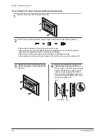
Страница 108: ...xternal devices prior to installing the wall bracket 5 The package contents and parts supplied for the wall mount are subject to change without prior notice 11 3 2 Parts Wall attachment panel is sold separately Plastic Hanger 4 Screw 4 1 Left 1 Right 1 Wall Mount Bracket ASSY HINGE Accessories 11 3 3 How to assemble the Wall Mount Bracket 1 The wall mount bracket is delivered separately Please tig...

Страница 109: ...e after hanging the SET on the wall mount bracket Please avoid catching your fingers while installing and adjusting the angle Please tightly secure the wall mount bracket to the wall to avoid injury from a falling SET 3 Tighten the screws of the plastic hanger shown in picture 2 to the back side of the PDP 4 Remove the Safety Pins Fasten the 4 plastic latches assembled at step on the back side of ...

Страница 110: ...ote To connect external devices such as a DVD or a Home Theater System to the PDP please refer to following instructions 1 Be sure to remove the safety pins underneath the PDP Note Note If the safety pins are not removed the angle cannot be adjusted Any attempt to do so may cause damage to the PDP 2 Hold onto the bottom of the PDP and pull forward fully as directed by the arrow as illustrated to a...

Страница 111: ...g Electronics 11 3 7 How to assemble the Stand Base 1 Pull the folded stand in the direction of the arrow Two or more people should carry the TV Never lay the TV on the floor because of possible damage to the screen Always store the TV upright Stand ...

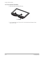
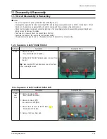
Страница 112: ...X Main Board Y Main Board etc A spark may be generated by the electric charge and there is danger of electronic shock Check that the cables are properly connected referring to the circuit diagram when disassembling or assembling the unit taking care not to damage the cables Take care not to cause a flaw in the Glass Filter in the front Assemble the boards in the reverse order of the disassembly Th...

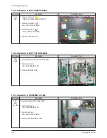
Страница 113: ...ZPC BLK Remove the Cover Rear 12 1 4 Separation of ASSY PCB MISC MAIN Part Name Description Description Photo Main Board Detach all connectors from the Main Board Remove 4 screws PH WWP M3 L8 NI PLT Remove the Main Board 12 1 5 Separation of FILTER EMI AC LINE Part Name Description Description Photo Filter EMI AC LINe Detach connector from Main SMPS Remove 2 screws PH WWP M3 L8 NI PLT Remove a scr...

Страница 114: ...escription Photo Bracket PCB Remove 2 screws BH S M4 L12 ZPC BLK Remove a screw BH S M4 L10 ZPC BLK Remove the BRACKET PCB 12 1 7 Separation of ASSY BOARD P SIDE AV Part Name Description Description Photo Side AV Remove a screw BH S M4 L10 ZPC BLK Remove a screw BH B M4 L12 ZPC BLK Remove the Side AV assy ...

Страница 115: ...tion Photo Power IR Board Remove 2 screws BH S M4 L8 ZPC BLK Remove the Power IR Board 12 1 8 Separation of ASSY SPEAKER P Part Name Description Description Photo Cover Rear Bottom Remove 9 screws BH B M4 L12 ZPC BLK Remove the Cover Rear Bottom Speaker Remove 4 screws BH WP B M4 0 L12 ZPC BLK SWRCH18A Remove the Speaker ...

Страница 116: ...ront cover 12 1 11 Separation of ASSY PCB P SMPS SMPS DC DC Part Name Description Description Photo SMPS SMPS DC DC Board Detach all connectors from the Assy PCB P SMPS Remove 8 screws PH WWP M3 L8 NI PLT Remove the Assy SMPS PCB Detach all connectors from the Assy SMPS DC DC Board Remove 4 screws PH WWP M3 L8 NI PLT Remove the SMPS DC DC Board Wear gloves when handling the power board as there ma...

Страница 117: ...ng Electronics 12 1 12 Separation of ASSY PDP MODULE P LOGIC MAIN BOARD Part Name Description Description Photo Logic Board Detach all connectors from the Logic Main Board Remove 4 screws WSP PH M3 L8 NI PLT Remove the Logic Main Board ...

Страница 118: ...DULE P X MAIN BOARD Part Name Description Description Photo Flat Cable Detach all Connectors from the X Main Board To separate the Flat Cable of the X Board press the upper and the lower sides of the connector X Main Board Remove 6 screws PH WWP M3 L8 NI PLT Remove the X Main Board ...

Страница 119: ...Name Description Description Photo Flat Cable Detach the 6 scan board connectors from the panel by pulling the holder from both the top and bottom ends Y Scan Remove 5 screws PH WWP M3 L8 NI PLT Connectors Separate the scan board from the Y Main Board by detaching the 3 connectors and remove the Scan Boards ...

Страница 120: ...Disassembly Reassembly Samsung Electronics 12 9 Part Name Description Description Photo Y Main Board Remove 8 screws PH WWP M3 L8 NI PLT Detach all connectors from the Y Main Board ...

Страница 121: ... PDP MODULE P ADDRESS BUFFER BOARD Part Name Description Description Photo Still Bar Remove 4 screws PH WWP M3 L8 NI PLT Remove the still bar Buffer Detach the all connectors from the buffer board Remove 12 screws PH WWP M3 L8 NI PLT Remove the E Board and F Board and G Board ...

Страница 122: ...UTPUTS Va Vg vs 3 4V turn off sequence Vca Vcs Keep Display ON w o display flicker while 3cycle full dip condition Standby step turn off for µ processor reset µ 1 When connecting the AC power cord Stand By 5V from the Main SMPS is supplied to the Main Board Pin 3 of CN1002 of Main Board 2 When pressing the Power button on the remote control or on the main body PS_ON Pin 5 of CN1002 of Main Board c...

Страница 123: ...than 300m ohm at the output short condition power circuit was designed to have the function of short over current protection O C P in all outputs Thus in condition of any over current in each output ports the power supply is shut down by O C P function for the protection of part s damage The specification about the O C P in each port is the same as following Table 2 Table 2 OCP specification Outpu...

Страница 124: ... state the relays RL8101 RL8102 are ON and input normal current flows through them without any overheat Sub Power Circuit Basic Operation This Stand by block is controlled by SMPS operation On off switching FET inside of PRC pulse ratio controlled IC STR V152 Using the switching operation we can get the energy in an input capacitor C8121 to transmit to output port for STD 5V dc source for Micom an...

Страница 125: ...we can get the higher power factor almost 1 0 in this power board Protection Function ㆍOver Voltage Protection Because the PFC controller IC UCC2818A has the function of over voltage protection about the high output voltage limit even if the overshoot and not controlled state occur with the deep condition in ac input source or output step load this controller protects the abnormal output voltage s...

Страница 126: ... Regulator Z8334 SI 3050J 25V 2 0A SANKEN Regulator RC8336 FMX 22S 200V 10A SANKEN Vamp Output Diode D8332 1SS244 250V 625mA ROHM Vt Output Diode RC8331 FMX 22S 200V 10A SANKEN Vg Output Diode RC8332 FMB 26L 60V 10A SANKEN 12V Output Diode Q8332 2SK2232 60V 25A TOSHIBA 6 5V Switching IC RC8333 RC8334 FMB 26L 60V 10A SANKEN 6 5V Output Diode Q8331 2SK3659 20V 65A NEC 5 3V Switching IC RC8335 FME 24...

Страница 127: ...Circuit Description 13 6 Samsung Electronics 13 2 2 PDP Module 1 Logic Board A name of main part of Logic Board and vocabulary ...

Страница 128: ...onnector to output the control signal for the Y drive board Operating Status LED The LED that shows whether the Sync and Clock signal is properly supplied to the logic board Normal Status Blinks at 0 5 second intervals LED2001 Lights up for 2 seconds at the initial operation and LED2002 flickers at an inter val of 0 5 seconds CN2010 CN2011 CN2012 The connector to output the address data and the co...

Страница 129: ... short test for each part If the Vref voltage Voltage Divider Voltage is lower than 1 25V check the resistance of the resistance output part and check if the circuit status is normal This applies the voltage and the proper Vref voltage and results in the screen being properly displayed If the screen is abnormally displayed even though the Vref voltage is normal find any abnormal points by conducti...

Страница 130: ...d That is the pixel whose wall charge has been formed by the Address Discharge forms a Sustain Discharge vis the following Sustain pulse 2 Sustain Discharge A Sustain Discharge is a Self Sustaining Discharge formed by the accumulation of the electric potential of the Sustain pulse gen erally 200 210 Volt alternating over the X and Y electrodes during the sustain period and the wall charge dependin...

Страница 131: ...k consists of 12 Scan Driver ICs TI SN755870 64 Outputs X Pole Terminal 4 Block Logic B d Logic G Buffer Sustain Pulse Energy Recovery Rising Ramp Pulse Falling Ramp Pulse Vscan Pulse Y Buffer Upper Y Buffer Lower Y Drive B d X Drive B d Sustain Pulse Energy Recovery Ve Bias Logic E Buffer Logic F Buffer Y Pole Terminal 6 Block Requisite Components Necessary for Drive Board Operation 1 Power Suppl...

Страница 132: ...FPC output electrodes sequentially one line at a time At this time Vscan is called the Scan Bias Voltage A Vscan voltage of approximately 175 Volt Vsc_1 is supplied to the electrode lines For the other lines 56 volt Vsc_h is higher than Vscan l by 120V is supplied However negative wall charges are accumulated on the Y electrode by the Ramp pulse and positive wall charges are accumulated on the add...

Страница 133: ...ance 0 2 When no signal is output to the gate GND FET changes to an open circuit i e an insulator of resistance High Voltage Switching of the FET Operation 1 When no signal is applied to G1 FET1 is opened and when the signal is applied to G2 FET2 short circuits GND is output via the output terminal 2 When a signal is applied to G1 FET1 short cir cuits and when no signal is applied to G2 FET2 is op...

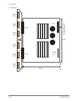
Страница 134: ...rcuit Description Samsung Electronics 13 13 Drive Board Connector Layout 1 X Main Board 190mm 380mm 1 VDD 2 VCC 3 DGND 4 DGND 5 Vb 6 DGND 7 DGND 8 Vs 9 Vs CN4004 CN4003 CN4002 CN4001 CN4000 CN4005 signal ...

Страница 135: ...ung Electronics 2 Y Main Board CN5502 Panel CN5503 Panel CN5501 Panel CN5403 Panel CN5402 Panel CN5401 Panel 265mm 320mm 1 Vs 2 Vs 3 GND 4 GND 5 Vset 6 GND 7 Vscan 8 GND 9 VCC 10 VDD CN5007 CN5008 signal CN5009 CN5010 CN5407 CN5507 ...

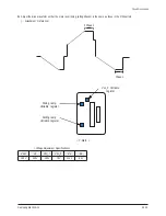
Страница 136: ...in reset rising falling 40usec is the same as those in the F W pattern Attachment 1 reference Voltage Adjustment Specifications Y Main 120usec 70usec Vsc_h Variable register Falling ramp Variable register Rising ramp Variable register Vset Vs Vsc_l Vsc_h Ve Va 190V 200V 190V 70V 115V 65V ...

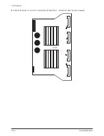
Страница 137: ...Circuit Description 13 16 Samsung Electronics Check that the output of X Out of the X board follows the waveform of Attachment 2 when the power is supplied X OUT ...

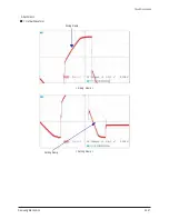
Страница 138: ...Circuit Description Samsung Electronics 13 17 Attachment 1 Y Output Waveform Rising Ramp Falling Ramp Rising Ramp Falling Ramp ...

Страница 139: ...Circuit Description 13 18 Samsung Electronics Scan_l Even_Scan Y Sustain ...

Страница 140: ...Circuit Description Samsung Electronics 13 19 Attachment 2 X Output Waveform X Sustain ...

Страница 141: ...13 20 Samsung Electronics MEMO ...

Страница 142: ...able is longer than for normal use check the visual quality of the video on the screen and shorten the length if necessary This also applies to the PC RGB D Sub cable When the length of the cable is longer than for normal use video may not be displayed on the screen In this case shorten the cable length When a digitally distributed TV user receives HD rated broadcasts The digital distributed TV Re...

Страница 143: ...ct ratio to normal 4 3 or wide 21 9 the left and right or top and bottom of the picture will not be displayed This symptom appears in other manufacturer s TV s The three appliance companies are trying to resolve the problem through the Ministry of Information and Communication In TV VIDEO S VIDEO and COMPONENT 480i 480p modes all screen modes can be selected 16 9 Zoom1 Zoom2 4 3 In TV DTV COMPONEN...

Страница 144: ...ng is a television broadcasting signal digitized and transmitted according to the United States terrestrial digital broadcast standard or ATSC Mono A type of audio interface that transmits the audio signal through a single channel only Through a mono interface it is hard to experience stereophonic sound and the sound is played using only one speaker Reception Sensitivity Amplification LNA A signal...

Страница 145: ...provide clearer and sharper visual quality Anynet Anynet is an AV network system that enables an easy to use AV interface for users by controlling all connected AV devices through the Anynet menu when the AV devices of Samsung Electronics are connected DVD Digital Versatile Disc DVD is a large capacity storage media that can store multime dia content such as video games audio applications etc usin...

Страница 146: ...hree primary colors of light R G and B the number of possible colors for a pixel is 256 x 256 x 256 16 777 216 or 16 7 million colors If 12 bits are used for a pixel the gradation is 212 or 4096 for a color Since three colors R G and B are used 4096 x 4096 x 4096 or 68 7 billion colors are support ed per pixel Since 68 7 billion colors are far more than 16 7 million colors the picture will be disp...

Страница 147: ...a of the signal broadcast from a broadcast station is smaller than that of possible color coordinates Moreover a TV provides a smaller color coordinate area than that of the signal from the broadcasting station even though the size of the color coordinate area varies depending on the TV model In general Color Reproductivity is used as follows The Color reproductivity of a TV is a certain of NTSC T...

Отзывы: