Circuit Description
13-8
Samsung Electronics
■
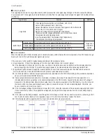
Normal Waveform
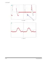
When the Operating LED blinks normally (at 0.5 second intervals), which indicates the normal operation of the PDP Set and Logic
Board, and the V-SYNC and data output signals are normal.
If the set is out of order, perform troubleshooting according to the procedures below.
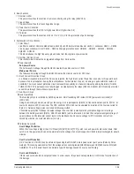
1) Visual Inspection : Check if the Operating LED on the Logic Main blinks at a 0.5 second interval.
▶
If the Operating LED blinks too fast or too slow, you have to reload the data onto the MICOM, as this indicates abnormal
data processing in the MICOM. To load the data, supply power to the module and load the data using GA-WRITER.
2) If no problem has been found through the visual inspection, check if the drive waveforms and the address data output are
normal. (Check Point: Check the DAMPING R-NET output of each data output terminal.)
▶
If no drive waveform or address output signal is detected, load data onto the MICOM according to the procedures described
above, as this indicates a MICOM data error.
▶
If data output is detected but is abnormal, it indicates a hardware short-circuit if measured for the drive waveform, or it
indicates abnormal data output due to the abnormal operation of the DDR memory caused by the abnormal Vref voltage if
measured in the address data. Abnormal data output due to the abnormal operation of the DDR memory or a short circuit on
the board, which may be caused during the ass'y process, causes the screen to be abnormally displayed. Therefore, you
have to conduct a short test for each part.
▶
If the Vref voltage (Voltage Divider Voltage) is lower than 1.25V, check the resistance of the resistance output part and check
if the circuit status is normal. This applies the voltage and the proper Vref voltage and results in the screen being properly
displayed.
▶
If the screen is abnormally displayed, even though the Vref voltage is normal, find any abnormal points by conducting a short
test. If a short circuit is found and it is repairable, repair it. If a short circuit is internal, replace the board.
▶
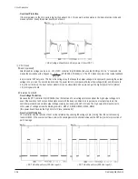
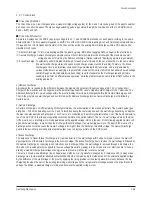
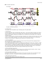
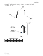
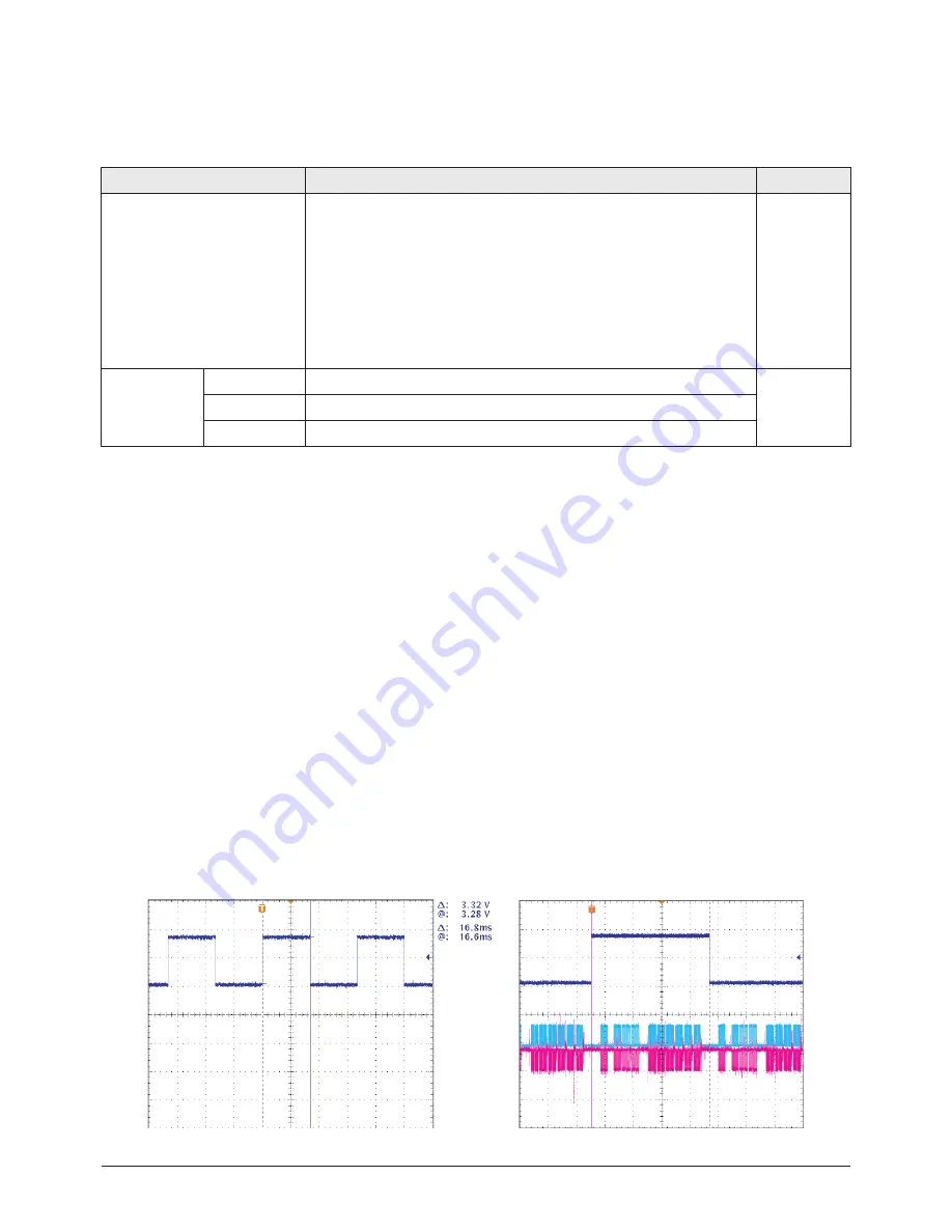
The following waveform appears when the V-sync and address data are output properly.
< Normal V-SYNC Output Waveform >
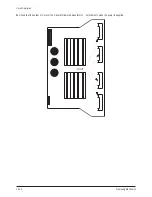
< Normal Address Data Output Waveform >
■
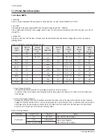
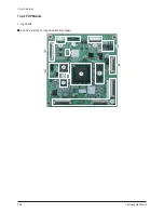
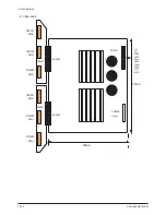
About Logic Board
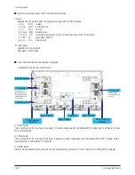
The Logic Board consists of a Logic Main board, which processes the video signal input through LVDS and creates the address
driver output and XY drive signals, and a Buffer board, which buffers the output signal and outputs the signal to the Address Driver
IC (TCP IC).
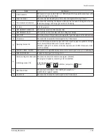
Logic Board
Function
Remark
Logic Main
- Video Signal Processing (W/L, error diffusion, APC, FCR)
Built-in LVDS Application and 1 ASIC Chip
- Outputs the Address Driver Control and Data Signals to the Buffer board
- Outputs the XY Drive Board Control Signal
- Major Drive Voltage Monitoring (MICOM Circuit Block)
: Detects abnormal voltage applications and protects drive circuits
- Temperature Induced Operating Mode
(Low Temperature/Room Temperature/High Temperature)
: Optimization of discharge by temperature
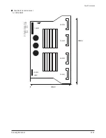
Buffer Board
E Buffer Board Outputs data and control signals to the bottom left TCP IC.
Single Scan
and RSDS
applied
F Buffer Board Outputs data and control signals to the center up TCP IC.
G Buffer Board Outputs data and control signals to the bottom right TCP IC.
Содержание HPS5033 - 50" Plasma TV
Страница 11: ...1 6 Samsung Electronics MEMO ...
Страница 47: ...3 30 Samsung Electronics MEMO ...
Страница 50: ...Samsung Electronics 5 2 MEMO ...
Страница 64: ...6 14 Samsung Electronics MEMO ...
Страница 68: ...Block Diagram 7 4 Samsung Electronics 7 2 3 Module Driver Board Block Diagram 1 Y Main Board 2 X Main Board ...
Страница 70: ...7 6 Samsung Electronics MEMO ...
Страница 139: ...Circuit Description 13 18 Samsung Electronics Scan_l Even_Scan Y Sustain ...
Страница 140: ...Circuit Description Samsung Electronics 13 19 Attachment 2 X Output Waveform X Sustain ...
Страница 141: ...13 20 Samsung Electronics MEMO ...


