20
Mar. 2008
GT-10
5.
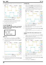
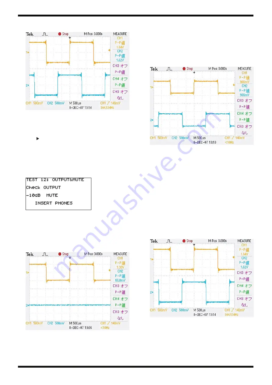
Verify that the waveform display on the oscilloscope is like that shown in
the figure below.
fig.11usbdout1.eps
Upper: left channel, lower: right channel
* The output level may vary according to the device capable of digital input.
6.
Subject the product to vibration and verify that no noise or other
abnormal sound is heard from the monitor speakers.
7.
Press [
] to advance to the next test.
12. OUTPUT&MUTE
Testing of SEND, PHONES, OUTPUT L/R, the MUTE
Circuitry for each output, and the OUTPUT -10/+4
dB Switching Circuitry
fig.12output&mute2e.eps
SEND Test
1.
Using a cable with a 1/4-inch phone plug, connect the
SEND
jack to
channel 1 on the oscilloscope and the left-channel monitor speaker.
2.
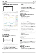
Verify that the output waveform display on the oscilloscope is as shown
in the figure below, and that no waveform is displayed while
MUTE
is
displayed on the screen.
fig.12out-send.eps
3.
Verify that the peak value is from
1.25
to
1.35 V
.
4.
Verify that signals are output from the monitor speakers and no noise or
other abnormal sound is heard, and that no sound is played while
MUTE
is displayed on the screen.
PHONES Test
1.
Using a cable with a 1/4-inch stereo phone plug (with 33-ohm load
resistor), connect the
PHONES
jack to channel 1 and channel 2 of the
oscilloscope and to the left-channel and right-channel monitor speakers.
2.
Verify that the
INSERT PHONES
message disappears from the screen.
3.
Verify that the output waveform display on the oscilloscope is what is
shown in the figure below, and that no waveform is displayed while
MUTE
is displayed on the screen.
fig.12out-phones.eps
Upper: left channel, lower: right channel
4.
Verify that the peak value for both the left and right channels is
0.95
to
1.05 V
(with 33-ohm load).
5.
Verify that signals are output from the monitor speakers and no noise or
other abnormal sound is heard, and that no sound is played while
MUTE
is displayed on the screen.
* Leave the a 1/4-inch stereo phone plug connected to the PHONES jack on the
GT-10.
Testing of OUTPUT L/R and the Monaural Jack
Switch
1.
Using the two cables with 1/4-inch phone plugs, connect the
OUTPUT L
and
R
jacks to channel 1 and channel 2 of the oscilloscope and to the left-
channel and right-channel monitor speakers.
2.
Verify that the output waveform display on the oscilloscope is what is
shown in the figure below, and that no waveform is displayed while
MUTE
is displayed on the screen.
fig.12out-out.eps
Upper: left channel, lower: right channel
3.
Verify that the peak value for both the left and right channels is
1.55
to
1.75 V
.
4.
Verify that signals are output from the monitor speakers and no noise or
other abnormal sound is heard, and that no sound is played while
MUTE
is displayed on the screen.
5.
Detach the plug from the
OUTPUT R
jack.
Содержание Boss GT-10
Страница 4: ...4 Mar 2008 GT 10 Location of Controls fig panel GT 10 eps...
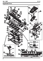
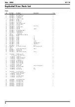
Страница 6: ...6 Mar 2008 GT 10 Exploded View fig bunkai eps L...
Страница 7: ...7 Mar 2008 GT 10 fig bunkai eps R...
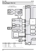
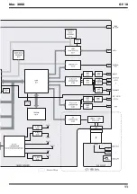
Страница 11: ...11 Mar 2008 GT 10 fig block wiring eps R...
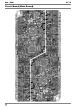
Страница 24: ...24 Mar 2008 GT 10 Circuit Board Main Board fig b main 1 eps...
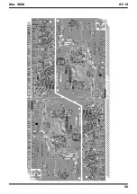
Страница 25: ...25 Mar 2008 GT 10 fig b main 2 eps...
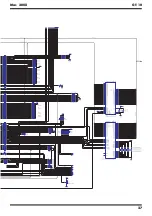
Страница 26: ...26 Mar 2008 GT 10 Circuit Diagram Main Board 1 5 fig d main 1 eps L...
Страница 27: ...27 Mar 2008 GT 10 fig d main 1 eps R...
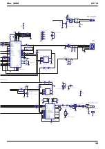
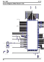
Страница 28: ...28 Mar 2008 GT 10 Circuit Diagram Main Board 2 5 fig d main 2 eps L...
Страница 29: ...29 Mar 2008 GT 10 fig d main 2 eps R...
Страница 30: ...30 Mar 2008 GT 10 Circuit Diagram Main Board 3 5 fig d main 3 e eps L...
Страница 32: ...32 Mar 2008 GT 10 Circuit Diagram Main Board 4 5 fig d main 4 eps L...
Страница 33: ...33 Mar 2008 GT 10 fig d main 4 eps R...
Страница 34: ...34 Mar 2008 GT 10 Circuit Diagram Main Board 5 5 fig d main 5 eps L...
Страница 35: ...35 Mar 2008 GT 10 fig d main 5 eps R...
Страница 36: ...36 Mar 2008 GT 10 Circuit Board SW VR Pedal Bank ENC EXP Board fig b sw 1 eps...
Страница 37: ...37 Mar 2008 GT 10 fig b sw 2 eps...
Страница 38: ...38 Mar 2008 GT 10 Circuit Diagram SW VR Board fig d sw vr eps L...
Страница 39: ...39 Mar 2008 GT 10 fig d sw vr eps R...
Страница 40: ...40 Mar 2008 GT 10 Circuit Diagram Pedal Board fig d pedal eps L...
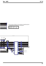
Страница 41: ...41 Mar 2008 GT 10 fig d pedal eps R...
Страница 42: ...42 Mar 2008 GT 10 Circuit Diagram Bank Board fig d bank eps Circuit Diagram ENC Board fig d enc eps...
Страница 44: ...MEMO Mar 2008 GT 10...

