


RF-WM-3200B1
Shenzhen RF-star Technology Co., Ltd.
Page 6 of 35
4.4.2.1 Pin Application Sample
4.5 Basic Operation of Hardware Design
4.6.1 Unsatisfactory Transmission Distance
........................................................................................ 29
4.7 Electrostatics Discharge Warnings
4.8 Soldering and Reflow Condition
Table of Figures
Figure 1. Functional Block Diagram of RF-WM-3200B1
............................................................................ 4
Figure 2. Part Number Conventions of RF-WM-3200B1
........................................................................... 4
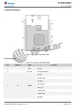
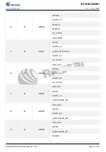
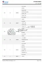
Figure 3. Pin Diagram of RF-WM-3200B1
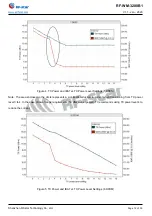
Figure 4. TX Power and IBAT vs TX Power Level Settings (1 DSSS)
................................................ 18
Figure 5. TX Power and IBAT vs TX Power Level Settings (6 OFDM)
............................................... 18
Figure 6. TX Power and IBAT vs TX Power Level Settings (54 OFDM)
............................................ 19
Figure 7. Photos of RF-WM-3200B1
Figure 8. Recommended PCB Footprint of RF-WM-3200B1 (mm)
..................................................... 22
Figure 10. Reference Schematic Diagram of RF-WM-3200B1
............................................................. 24
Figure 11. Pin Application Example of RF-WM-3200B1
........................................................................... 25
Figure 12. Recommendation of Antenna Layout
......................................................................................... 29
Figure 13. Recommended Reflow for Lead Free Solder
......................................................................... 31


