RF-Star RF-WM-3200B1 Скачать руководство пользователя страница 29


RF-WM-3200B1 

www.szrfstar.com

                                                                                                                                                    V1.1 - Jan., 2020 

Shenzhen RF-star Technology Co., Ltd.                                                                                                                   

Page 28 of 35


4.5 Basic Operation of Hardware Design 

1.  It is recommended to offer the module with a DC stabilized power supply, a tiny power supply ripple coefficient and 

the reliable ground. Please pay attention to the correct connection between the positive and negative poles of the 

power supply. Otherwise, the reverse connection may cause permanent damage to the module; 

2.  Please ensure the supply voltage is between the recommended values. The module will be permanently damaged 

if  the  voltage  exceeds  the  maximum  value.  Please  ensure  the  stable  power  supply  and  no  frequently  fluctuated 

voltage. 

3.  When  designing  the  power  supply  circuit  for  the  module,  it  is  recommended  to  reserve  more  than  30%  of  the 

margin, which is beneficial to the long-term stable operation of the whole machine. The module should be far away 

from  the  power  electromagnetic,  transformer,  high-frequency  wiring  and  other  parts  with  large  electromagnetic 

interference. 

4.  The bottom of module should avoid high-frequency digital routing, high-frequency analog routing and power routing. 

If it has to route the wire on the bottom of module, for example, it is assumed that the module is soldered to the Top 

Layer,


the copper must be spread on the connection part of the top layer and the module, and be close to the digital 

part of module and routed in the Bottom Layer (all copper is well grounded).   

5.  Assuming  that the module  is  soldered or placed  in  the Top Layer, it is  also wrong  to randomly  route  the Bottom 

Layer or other layers, which will affect the spurs and receiving sensitivity of the module to some degrees; 

6.  Assuming  that  there  are  devices  with  large  electromagnetic  interference  around  the  module,  which  will  greatly 

affect the module performance. It is recommended to stay away from the module according to the strength of the 

interference. If circumstances permit, appropriate isolation and shielding can be done. 

7.  Assuming that there are routings of large electromagnetic interference around the module (high-frequency digital, 

high-frequency analog, power routings), which will also greatly affect the module performance. It is recommended 

to stay away from the module  according to the strength of the interference. If circumstances permit, appropriate 

isolation and shielding can be done. 

8.  It is recommended to stay away from the devices whose TTL protocol is the same 2.4 GHz and 5 GHz physical 

layer, for example: USB 3.0. 

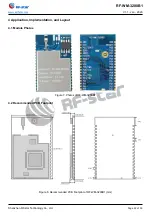
9.  The antenna installation structure has a great influence on the module performance. It is necessary to ensure the 

antenna is exposed and preferably vertically upward. When the module is installed inside of the case, a high-quality 

antenna extension wire can be used to extend the antenna to the outside of the case. 

10.  The antenna must not be installed inside the metal case, which will cause the transmission distance to be greatly 

weakened. 

11.  The recommendation of antenna layout. 

The chip antenna position on PCB is free space electromagnetic radiation. The location and layout of antenna is a 

key factor to increase the data rate and transmission range. 

Содержание RF-WM-3200B1

Страница 1: ...RF WM 3200B1 Low Power Wi Fi Module Version 1 1 Shenzhen RF star Technology Co Ltd Jan 19th 2020...

Страница 2: ...20 31 100 RF WM 3200B1I 1M IPEX 20 31 150 Conta ct Me RF WM 3200B2 16M Chip 20 31 100 RF WM 3200B3 1M Half hole 20 5 17 5 100 CC3220 M4 256 17 RF WM 3220B1 4M Chip IPEX 20 31 100 RTL8710AF M3 512 17 R...

Страница 3: ...or antenna integration including surface mounted chip antenna an IPEX interface for connecting an external antenna and a RF pad for soldering onto the base board and routing to an on board antenna RF...

Страница 4: ...Wi Fi provisioning TX power 18 0 dBm 1 DSSS 14 5 dBm 54 OFDM RX sensitivity 95 7 dBm 1 DSSS 74 0 dBm 54 OFDM Application throughput UDP 16 Mbps TCP 13 Mbps Power Management Subsystem Integrated DC DC...

Страница 5: ...umbers are of the form of RF WM 3200B1 where the fields are defined as follows Figure 2 Part Number Conventions of RF WM 3200B1 GPIO s Reset Band Pass Filter 40 0 MHz 32 768 kHz CC3200 Half hole Inter...

Страница 6: ...ctions 8 2 1 Module Parameters 8 2 2 Module Pin Diagram 9 2 3 Pin Functions 9 3 Specifications 15 3 1 Absolute Maximum Ratings 15 3 2 Recommended Operating Conditions 15 3 3 RF Parameters 16 3 3 1 Cur...

Страница 7: ...unctional Block Diagram of RF WM 3200B1 4 Figure 2 Part Number Conventions of RF WM 3200B1 4 Figure 3 Pin Diagram of RF WM 3200B1 9 Figure 4 TX Power and IBAT vs TX Power Level Settings 1 DSSS 18 Figu...

Страница 8: ...2 Pin Functions of RF WM 3200B1 9 Table 3 Absolute Maximum Ratings 15 Table 4 Recommended Operating Conditions of RF WM 3200B1 15 Table 5 Table of Current Consumption 16 Table 6 WLAN Receiver Charact...

Страница 9: ...dBm 1 DSSS 14 5 dBm 54 OFDM Receiving Sensitivity 95 7 dBm 1 DSSS 74 0 dBm 54 OFDM GPIO 29 Power Consumption Hibernate 4 A Low power deep sleep LPDS 250 A Idle connected MCU in LPDS 825 A DTIM 1 RX tr...

Страница 10: ...Page 9 of 35 2 2 Module Pin Diagram Figure 3 Pin Diagram of RF WM 3200B1 2 3 Pin Functions Table 2 Pin Functions of RF WM 3200B1 Pin Chip Pin Name Function 1 GND Ground 2 RF_OUT RF output interface 3...

Страница 11: ...IO30 UART0_TX McACLK McAFSX GT_CCP05 GSPI_MISO 5 55 GPIO01 GPIO1 UART0_TX pCLK Pixel PIXCLK UART1_TX GT_CCP01 6 57 GPIO02 ADC_CH0 GPIO2 UART0_RX UART1_RX GT_CCP02 7 58 GPIO03 ADC_CH1 GPIO3 UART1_TX pD...

Страница 12: ...GPIO06 GPIO6 UART0_RTS pDATA4 CAM_D0 UART1_CTS UART0_CTS GT_CCP06 11 62 GPIO07 GPIO7 McACLKX UART1_RTS UART0_RTS UART0_TX 12 63 GPIO08 GPIO8 SDCARD_IRQ McAFSX GT_CCP06 13 64 GPIO09 GPIO9 GT_PWM05 SDCA...

Страница 13: ...SDA GT_PWM07 pXCLK XVCLK SDCARD_CMD UART1_RX GT_CCP02 McAFSX 16 3 GPIO12 GPIO12 McACLK pVS VSYNC I2C_SCL UART0_TX GT_CCP03 17 4 GPIO13 GPIO13 I2C_SDA pHS HSYNC UART0_RX GT_CCP04 18 5 GPIO14 GPIO14 I2C...

Страница 14: ...GPIO16 GPIO16 GSPI_MOSI pDATA10 CAM_D6 UART1_TX GT_CCP07 SDCARD_CLK 21 8 GPIO17 GPIO17 UART1_RX GSPI_CS pDATA11 CAM_D7 SDCARD_CMD 22 15 GPIO22 GPIO22 McAFSX GT_CCP04 23 16 JTAG TDI TDI GPIO23 UART1_TX...

Страница 15: ...MS GPIO29 28 29 ANTSEL1 I O 29 30 ANTSEL2 I O 30 32 RESET Module reset pin internal pull up by default active low 31 45 DCDC_ANA2 GPIO31 UART0_RX McAFSX UART1_RX McAXR0 GSPI_CLK DCDC_ANA2_SW_P 32 35 S...

Страница 16: ...emperature 55 25 125 3 2 Recommended Operating Conditions Over operating free air temperature range unless otherwise noted 1 2 Table 4 Recommended Operating Conditions of RF WM 3200B1 Items Condition...

Страница 17: ...e TX 1 DSSS TX power level 0 278 mA TX power level 4 194 mA 6 OFDM TX power level 0 254 mA TX power level 4 185 mA 54 OFDM TX power level 0 229 mA TX power level 4 166 mA RX 1 DSSS 59 mA 54 OFDM 59 mA...

Страница 18: ...system The active current numbers scale based on the VBAT voltage supplied 3 DTIM 1 4 LPDS current does not include the external serial flash The LPDS number reported is with retention of 64 KB MCU S...

Страница 19: ...Level Settings 1 DSSS Note The area enclosed in the circle represents a significant reduction in current when transitioning from TX power level 3 to 4 In the case of lower range requirements 14 dbm o...

Страница 20: ...Test The transmission distance test was conducted in the outdoor open area and four RF WM 3200B1 modules were divided into two groups for Socket communication Module A1 operates in STA mode and modul...

Страница 21: ...tenna modules Wi Fi Module Sending Packet Receiving Packet Number of Packet Loss Packet Loss Rate A2 Module UDP Client B2 Module UDP Server 1392 1351 41 2 9 A2 Module UDP Client B2 Module UDP Server 1...

Страница 22: ...ble 7 WLAN Transmitter Characteristics TA 25 C VBAT 2 7 V to 3 6 V Parameters measured at SoC pin on channel 7 2442 MHz Parameter Conditions Mbps Min Typ Max Unit Maximum RMS Output Power Measured at...

Страница 23: ...1 Jan 2020 Shenzhen RF star Technology Co Ltd Page 22 of 35 4 Application Implementation and Layout 4 1 Module Photos Figure 7 Photos of RF WM 3200B1 4 2 Recommended PCB Footprint Figure 8 Recommended...

Страница 24: ...eter Antenna C27 C30 C31 L7 Chip Antenna 1 pF NC NC 1 8 nH External Antenna Interface NC 0 NC NC The module uses the onboard ceramic antenna by default If you need to use an external antenna please sw...

Страница 25: ...into Flash via UART0_TX and UART0_RX 2 When J15 J16 and J17 are disconnected the module is in the functional mode 4 Wire JTAG mode 3 When Pin 1 2 of J17 are shorted connected and J15 and J16 are disco...

Страница 26: ...echnology Co Ltd Page 25 of 35 Figure 11 Pin Application Example of RF WM 3200B1 The functions of IO ports can be configured flexibly and the program is generated easily by the program Pin Mux offered...

Страница 27: ...an 2020 Shenzhen RF star Technology Co Ltd Page 26 of 35 Select GPIO and click Add Remove the select of GPIO Signals Select GPIO2 and GPIO5 and choose the corresponding IO type Select UART and click A...

Страница 28: ...Page 27 of 35 As the pin numbers of GPIO03 and GPIO04 are 58 and 59 respectively just select the corresponding pin as shown After configuration is done click Generate to generate c and h files Add th...

Страница 29: ...ule is soldered or placed in the Top Layer it is also wrong to randomly route the Bottom Layer or other layers which will affect the spurs and receiving sensitivity of the module to some degrees 6 Ass...

Страница 30: ...ence will lead to an increase in communication packet loss rate The performances of ground absorption and reflection of radio waves will be poor when the module is tested close to the ground 2 Seawate...

Страница 31: ...trostatics Discharge Warnings The module will be damaged for the discharge of static RF star suggest that all modules should follow the 3 precautions below 1 According to the anti static measures bare...

Страница 32: ...0 s 90 s 30 s 90 s Peak Temperature Tp 220 235 230 250 Average Descend Rate Tp to Tmax Max 6 s Max 6 s Time from 25 to Peak Temperature t2 Max 6 minutes Max 8 minutes Time of Soldering Zone tP 20 10 s...

Страница 33: ...RF WM 3200B1 www szrfstar com V1 1 Jan 2020 Shenzhen RF star Technology Co Ltd Page 32 of 35 5 Certification 5 1 RoHS RoHS Report No DTI201805214715 Figure 15 RoHS certificate...

Страница 34: ...1 0 3 Modify product photo Eaton 2016 07 06 V1 0 4 Add side view of the module Eaton 2016 07 25 V1 0 5 Add optional antenna chapter Eaton 2016 09 22 V1 0 6 Modify module model Eaton 2019 09 20 V1 1 En...

Страница 35: ...OGY CO LTD Shenzhen HQ Add Room 601 Block C Skyworth Building High tech Park Nanshan District Shenzhen Guangdong China Tel 86 755 3695 3756 Chengdu Branch Add No B3 03 Building No 1 Incubation Park Hi...

Отзывы: