background image

TPS-1 User’s Manual: Hardware 


5. TPS-1 boot subsystem 

R19UH0081ED0107 Rev. 1.07 


page  44  of 86 

Jul 30, 2018


5.2.  Loading and update of the firmware during the manufacturing process 

The serial boot Flash can be written in several ways: 


before mounting with a programmer, 


via JTAG interface

Note1


via serial interface (UART)

Note1


via ETHERNET interface (BOOTP/TFTP)

Note2


Note 

Basically we recommend to use serial interface (UART) during the development phase to fill an empty Flash. 


via ETHERNET is for firmware update only. If you have TPS-1 toolkit v1.1.0.2 or later, please pre-program empty Flash with “default 

image” in the toolkit before the Flash is soldered. It allows to do all required setting via ETHERNET. 


5.2.1.  UART interface (UART boot) 

The UART interface is used for basic communication with the TPS-1. The interface is reduced to a minimum and has no modem lines.   


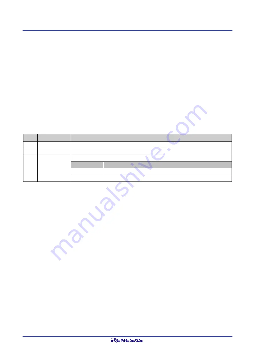
Table 5-1: Boot UART lines 

Pin 

Signal TPS-1 

Description 

C14 

UART6_TX 

Boot UART “Transmit data” 

C13 

UART6_RX 

Boot UART “Receive data” 

P12 

BOOT_1 

Forced Boot 

Value 

Function 

0x0 

BROM: Boot from Boot Flash is enabled (normal operating mode). 

0x1 

UART: Boot via UART is enabled. 


The signal line BOOT_1 (Forced Boot) forces a firmware update. For this update, the UART interface is used. In this case also a corrupt version can be 

updated. 


The following parameters are set (fix) for the Interface: 


Baudrate: 115200 baud 


8-bit data length 


1 stop bit 


no parity check 


no hardware flow control 

Содержание TPS-1

Страница 1: ...is subject to change by Renesas Electronics Corp without notice Please review the latest information published by Renesas Electronics Corp through various means including the Renesas Electronics Corp website http www renesas com TPS 1 User s Manual Hardware Rev 1 07 Jul 2018 RENESAS ASSP Ethernet Controller for PROFINET IO Devices User s Manual www renesas com ...

Страница 2: ...onics with respect to maximum ratings operating power supply voltage range heat dissipation characteristics installation etc Renesas Electronics disclaims any and all liability for any malfunctions failure or accident arising out of the use of Renesas Electronics products outside of such specified ranges 7 Although Renesas Electronics endeavors to improve the quality and reliability of Renesas Ele...

Страница 3: ...d product where the reset signal is applied to the external reset pin the states of pins are not guaranteed from the moment when power is supplied until the reset process is completed In a similar way the states of pins in a product that is reset by an on chip power on reset function are not guaranteed from the moment when power is supplied until the power reaches the level at which resetting has ...

Страница 4: ... 1 Make sure to refer to the latest versions of these documents The newest versions of the documents listed may be obtained from the Renesas Electronics Web site Document Type Description Document Title Document No Data Sheet Hardware overview and electrical characteristics TPS 1 Datasheet R19DS0069EJ User s manual for Hardware Hardware specifications pin assignments memory maps peripheral functio...

Страница 5: ...itter Coupled Logic PLL Phase Locked Loop POF Plastic Optical Fiber POR Power On Reset RJ 45 Ethernet connection copper wire SC RJ Ethernet connection fiber optic SPI Serial Peripheral Interface UART Universal Asynchronous Receiver Transmitter n c Not connected ppm Parts per Million Abbreviation Full Form AR Application Relation PROFINET terms CR Communication Relation PROFINET terms I M Identific...

Страница 6: ... EVENT COMMUNICATION WITH THE TPS 1 FIRMWARE 36 4 2 EVENTS FROM THE TPS 1 FIRMWARE TO THE HOST 37 4 3 EVENTS FROM THE HOST TO THE TPS 1 FIRMWARE 38 4 4 INTERRUPT COMMUNICATION WITH THE TPS 1 39 4 4 1 How to generate an interrupt by an event 39 5 TPS 1 BOOT SUBSYSTEM 43 5 1 HARDWARE STRUCTURE FOR THE BOOT OPERATION 43 5 2 LOADING AND UPDATE OF THE FIRMWARE DURING THE MANUFACTURING PROCESS 44 5 2 1 ...

Страница 7: ... 69 Configuration of the IO Local Parallel Interface 69 Configuration of the IO Local Serial interface SPI Master 70 I M0 Configuration I M0 data Deleted OK 71 ETHERNET INTERFACE CONFIGURATION 72 COPYING THE CONFIGURATION DATA INTO THE BOOT FLASH 73 GENERATING A COMPLETE SERIAL BOOT FLASH IMAGE 74 BOARD DESIGN INFORMATION 75 VOLTAGE SUPPLY 75 SWITCHING REGULATOR 75 Wiring for the Switching Regulat...

Страница 8: ...gotiation Auto Cross Over Auto Polarity Support for 100Base TX and 100Base FX ports Monitoring of fiber optic transmission links with integrated I2 C interfaces Power dissipation around 1 W Host Interface Serial SPI up to 25 MHz and parallel 8 or 16 bit interface for use with an external host CPU Data exchange cyclic and acyclic with external host via integrated Shared Memory Area event and interr...

Страница 9: ...ynchronization tasks To support line topologies in PROFINET networks the TPS 1 is equipped with two integrated PHYs and an integrated IRT switch Time critical PROFINET protocols are supported by hardware For the complete implementation of a PROFINET device interface only the TPS 1 a serial Flash device an oscillator and the physical adaptations for the Ethernet interface transformers and connector...

Страница 10: ...ink2 Act2 Test Sync JTAG Debug Serial Flash SPI Slave Host Interface Parallel Serial 48 GPIO Status Info LEDs Control Signals Power Supply Switching Regulator 3 3 V 1 5 V Figure 1 2 TPS 1 Block Diagram The TPS 1 contains the PROFINET CPU the PROFINET core the I O interface and the Host Interface for connecting a host CPU The PROFINET core processes the PROFINET communication All time critical serv...

Страница 11: ...LED Bus Failure active low B11 LED_SF_OUT O Control LED System Fail active low C10 LED_READY_OUT O Control LED Device Ready active low B10 LED_MT_OUT O Control LED Maintenance active low PHY Port 1 C9 I2C_1_D_INOUT I O Fiber Optic Port 1 I2 C Bus Data e g SC RJ C6 SCLK_1_INOUT O Fiber Optic Port 1 I2 C Bus Clock e g SC RJ C12 LINK_PHY1 O LINK indication ETHERNET Port 1 up or down active high D10 A...

Страница 12: ...L4 TM0 I Test Input 0 Chip Test 10k to GND pull down external J10 TM1 I Test Input 1 Chip Test 10k to GND pull down external K5 TRSTN I JTAG Interface Test Reset pull down external L6 TMS I JTAG Interface Test Mode Select pull up external L7 TDO O JTAG Interface Test Data Output J5 TCK I JTAG Interface Test Clock pull up external L5 TDI I JTAG Interface Test Data Input pull up external Reset Test ...

Страница 13: ...upply Port 2 H14 VDDACB I Analog 3 3 V VDD must be generated via a filter from digital 3 3 V power supply G13 VSSAPLLCB Analog central GND G14 VDDAPLL Analog central power supply for PHYs 1 5 V Pins for core PLL power supply L9 PLL_AGND PLL analog GND core PLL L10 PLL_AVDD PLL analog 1 0 V core PLL Pins for switching regulator J1 BVDD I Supply voltage for the switching regulator 3 3 V supply for t...

Страница 14: ...GPIO 30 LBU A8 IN Address Bit K2 GPIO 31 LBU A9 IN Address Bit L2 GPIO 32 LBU A10 IN Address Bit L3 GPIO 33 LBU A11 IN Address Bit L1 GPIO 34 LBU A12 IN Address Bit M2 GPIO 35 LBU A13 IN Address Bit M1 GPIO 36 LBU SEG0 IN Segment choice 1 M3 GPIO 37 LBU SEG1 IN Segment choice 2 P3 GPIO 38 HOST RESET IN Reset Host SPI Interface N3 GPIO 39 HOST SFRN IN Start new SPI Transfer Note 3 N2 GPIO 40 HOST S...

Страница 15: ...ower supply 1 5 V PHY H14 VDDACB Analog central power supply 3 3 V PHY Must be generated from VDD33 via a filter E12 VDD33ESD Analog test power supply 3 3 V PHY G13 VSSAPLLCB Analog central GND PHY Must be generated from GND Core IO via a filter or connected to GND Core IO at the far end from TPS 1 C8 M8 VDDQ_PECL_B1 VDDQ_PECL_B2 PECL buffer power supply 3 3 V port 1 and port 2 L9 PLL_AGND Analog ...

Страница 16: ... Pin Function Comment TEST_SYNC N12 Start of bus cycle A signal on this pin signalizes a new cycle event It is used as well to test the synchronization during the certification The signal should be made accessible for measurement purposes T1 J11 Ti T_IO_Input Time at which the input data must be read from process T2 H11 To T_IO_Output Data can be used by the application at this configured time T3 ...

Страница 17: ...e time 3 1 Testing DPRAM Interface For testing the DPRAM Interface it is useful to have addresses with defined values After start of the TPS 1 firmware the TPS 1 writes the magic number and the NRT Area Size into the addresses 0x8000 and 0x8004 TPS 1 0x8000 0x8004 0x0000 0xFFFF Magic Number NRT Area Size ARM CPU Application CPU The application CPU read the Magic Number to recognize the start up of...

Страница 18: ...ress bits to the signals LBU_SEG0_IN and LBU_SEG1_IN see Table 3 2 Figure 3 2 and Figure 3 3 LBU_Ax_IN 13 0 A 15 0 A 13 0 A 15 14 Ext Host CPU Figure 3 2 TPS 1 with address page 16 Kbyte You can also choose a page size of 4 Kbyte When you choose 4 Kbyte pages you have less space inside the NRT area for configuration slots and subslots LBU_Ax_IN 15 14 LBU_Ax_IN 11 0 A 13 0 A 11 0 A 13 12 Ext Host C...

Страница 19: ...0 LBU_DATA15 data line 0 15 LBU_A0_IN LBU_A13_IN Address lines 0 13 LBU_SEG0_IN Low Bit of the segment page selection LBU_SEG1_IN High Bit of the segment page selection During a memory access the TPS 1 behaves like a 16 bit Little Endian device with an 8 bit or 16 bit memory The possible access types are listed in Table 3 3 Table 3 3 16 Bit External Host Databus LBU_BE_2_IN LBU_BE_1_IN Access type...

Страница 20: ...he LBU_SEGx_IN signals Table 3 5 shows the page decoding Table 3 5 Page selection with LBU_SEGx_IN signals LBU_SEG 1 0 Selected Page 0 0 Page 00 0 1 Page 01 1 0 Page 02 1 1 Page 03 The segmentation with 16 Kbyte pages is shown in Figure 3 4 With 16 address lines you can reach the whole 64 kByte address space 0x0000 0x2000 0x8000 0xFFFF NRT Area IO RAM Event Unit 16 K Page Size 0x4000 0xC000 Page 0...

Страница 21: ...te Event Unit and the complete IO RAM Out of the NRT area you can only use the address space between 0x8000 and 0x9FFF 0x0000 0x2000 0x8000 0xFFFF NRT Area IO RAM Event Unit 4 K Page Size 0x3000 0x9000 Page 00 Page 02 Page 01 Page 03 0x1000 0x9FFF Figure 3 5 4 kByte page size Because of the page size it is not possible to use the max Possible number of slots and subslots Other page sizes than 16 k...

Страница 22: ...ection example of an 8 bit data bus to the TPS 1 TPS 1 HOST CPU RDN A0 A15 CSN AD0 AD7 A14 A15 WR0N LBU_CS_IN LBU_BE_1_IN LBU_BE_2_IN LBU_READ_EN_IN LBU_SEG0_IN LBU_SEG1_IN LBU_WR_EN_IN LBU_A0_IN LBU_A13_IN LBU_DATA0 LBU_DATA7 WR0N byte RDN AD0 AD7 A0 A15 0 0 0 INTN INT_OUT INT Port READYN LBU_READY_OUT WAITN 1 CSN Figure 3 6 Connection example for an 8 bit data bus ...

Страница 23: ... address space of 64 KByte Address line A0 should not be connected using the 16 bit data bus The Address line LBU_A0_IN should be connected to a pull down TPS 1 HOST CPU RDN A1 A15 CSN AD0 AD15 A14 A15 WR0N WR1N LBU_CS_IN LBU_BE_1_IN LBU_BE_2_IN LBU_READ_EN_IN LBU_SEG0_IN LBU_SEG1_IN LBU_WR_EN_IN LBU_A1_IN LBU_A13_IN LBU_DATA0 LBU_DATA15 WR0N WR1N RDN AD0 AD15 A1 A15 0 0 0 INTN INT_OUT INT Port RE...

Страница 24: ...rial Clock Input Serial Clock driven by the SPI Master M4 GPIO_42 HOST_STXD_OUT Serial Data Output MISO Master in Slave out P4 GPIO_43 HOST_SHDR_OUT Serial Header Information header information available An unknown or wrong SPI access causes an Error IRQ that is reported to the host CPU by the event unit The clock phase and the CPOL clock polarity is adjustable active low active high The following...

Страница 25: ... SPI slave As long as the chip select signal is active data are exchanged between the devices master slave 3 3 1 1 Header structure The content and meaning of SPI data is defined by the implementation of the SPI slave The following chapter describes the structure of the SPI slave commands Table 3 7 SPI header structure Header Data Byte 0 Byte 1 Byte 2 Byte 3 Byte 4 Byte 5 max Command Address Addre...

Страница 26: ...e 3 9 Command byte for SPI slaves host interface The bits of the command byte have the following meaning b7 indicates a read command b6 indicates a write command b5 and b4 describe the addressing range 00 MEM access to the complete shared memory 64 Kbyte 01 IO access to the input output area 10 access to a multicast provider CR only write 11 fractional access to an I CR b6 1 or MC CR b6 0 b3 b0 co...

Страница 27: ...es Read MEM Direct Reads from the transferred address The length is coded in the command byte 0b1000_nnnn 0x8n 2 0 1 15 Write MEM Direct Writes to the transferred address The length is coded in the command byte 0b0100_nnnn 0x4n 2 0 1 15 MEM Access With this command the external host CPU can read from and write to the complete 64 Kbyte address space with a maximum data length of 64 Kbyte access to ...

Страница 28: ...ittle Endian format by the serial host interface When connecting a Big Endian Host System the format has to be changed into the correct order There is a maximum clock frequency of 25 MHz possible using this interface B7 B6 B5 B4 B3 B1 B2 B0 B15 B14 B13 B12 B11 B9 B10 B8 B7 B6 B5 B4 HOST_SCLK_IN SPI Header SPI Data B7 B6 B5 B4 B3 B1 B2 B0 B15 B14 B13 B12 B11 B9 B10 B8 Dumm y Dumm y Dumm y Dumm y MS...

Страница 29: ...IN signal is required to synchronize bytes transferred to the TPS 1 with the peripheral interface The timing to be observed can be seen in Figure 3 11 T1 T2 and T3 The timing is based on the system clock of the TPS 1 100 MHz 10 ns it must as well be applied in the situations shown in Figure 3 12 Figure 3 13 and Figure 3 14 Table 9 Timing HOST_SFRN_IN signal Phase Timing Description T1 min 1 system...

Страница 30: ... slave interface can transmit the requested data the HOST_STRX_OUT signal is set to its active level This indicates to the SPI master that it can start the next cycle and the master release the Busy_Enable signal This forces the SPI slave to release the Busy level and the master starts the next clock cycle B23 B22 B21 B20 B19 B17 B18 B16 HOST_SCLK_IN HOST_SFRN_IN HOST_SRXD_IN B9 B10 B8 B9 B10 B8 D...

Страница 31: ...B17 B18 B16 HOST_SCLK_IN HOST_SFRN_IN HOST_SRXD_IN B9 B10 B8 B9 B10 B8 Dummy Dummy Dummy Dummy Dummy Dummy Dummy Dummy B7 B6 B5 B4 B3 Dummy Dummy Dummy Dummy Dummy HOST_STXD_OUT SPI Status SPI RD Data Motorola SPI format SPO 0 SPH 0 Wait_Time Figure 3 14 SPI Read Timing Wait Mode The following equation describes the Wait Time after the command bytes before starting the payload data TWait 32 fsys f...

Страница 32: ...re shows two SPI transfers each 5 byte long and the wait time between this cycles e g TPS_GetValue16 e g TPS_GetValue16 HOST_SCLK_IN Wait Time between two SPI transfers L 1 Data transfer HOST_SRXD_IN HOST_STXD_OUT CMD Byte ADR Byte ADR Byte Data Byte Data Byte CMD Byte ADR Byte ADR Byte Data Byte Data Byte CMD Byte ADR Byte ADR Byte Data Byte Data Byte CMD Byte ADR Byte ADR Byte Data Byte Data Byt...

Страница 33: ...UT B15 B14 B13 B12 4 x SysCLK B7 B6 B5 B4 B3 B2 B1 B0 B7 B6 B5 B4 B3 B2 B1 B0 HOST_RESET_IN SPI Data MSBit LSBit Dummy Dummy Dummy Dummy Dummy Dummy Dummy Dummy Dummy Dummy Figure 3 16 SPI Slave Reset Timing The signal HOST_RESET_IN is the only way to set the slave interface to a defined status The signal is active high During the normal operation the signal is set to low level If you want to ensu...

Страница 34: ...NRT Area up to 0x9FFF 0x0000 0x2000 0x2800 0x8000 reserved reserved Output Area Input Area MC Provider Area 2k Byte TPS 1 Information Area Device Vendor Information RecordMailbox Supervisor AR 0xFFFF IO RAM NRT Area 32k Byte Event and IO area 32k Byte Slot Subslot configuration reserved TCP IP Mailbox AR0 RecordMailbox AR0 AlarmMailbox high AR0 AlarmMailbox low AR1 RecordMailbox AR1 AlarmMailbox h...

Страница 35: ...e memory area shared memory is used for the access to acyclic and cyclic data The size depends on the device Exchange of the cyclic data is managed in the peripheral interface input output area The structure of this area is fixed It is possible to manage one AR Application Relations in the first release one I Data CR one O Data CR The IO data has a maximum size of 1016 Byte cyclic data dynamically...

Страница 36: ...ss changes of the event register the TPS 1 and the host CPU has to poll these registers You can also use an interrupt control mode if the host CPU supports this The event bits corresponding to the mail box access are not ambiguous After receiving this event it is necessary to check each mail box In the header of the respective mail box the READ_FLAG is set The following tables describe the structu...

Страница 37: ...when an alarm low priority is acknowledged from the controller TPS_EVENT_ONDIAG_ACK Set if a diagnostic alarm is acknowledged TPS_EVENT_ONCONNECT_REQ_REC_0 Set if a Connect Req for the first AR AR0 is received TPS_EVENT_ONCONNECT_REQ_REC_1 Set if a Connect Req for the first AR AR1 is received TPS_EVENT_ONCONNECT_REQ_REC_2 Set if a Connect Req for the third AR AR2 is received TPS_EVENT_ON_SET_DEVNA...

Страница 38: ...nnect Request of the AR1 APP_EVENT_ONCONNECT_OK_2 Connect AR2 ok Is set after the host processes the Framelayout Parameter out of a Connect Request of the AR2 APP_EVENT_ABORT_AR_0 AR0 is disconnected by the host APP_EVENT_ABORT_AR_1 AR1 is disconnected by the host APP_EVENT_ABORT_AR_2 AR2 is disconnected by the host APP_EVENT_PULL_SUBMODULE A submodule is pulled out of the device APP_EVENT_RETURN_...

Страница 39: ...register to reset the interrupt pin INT_OUT It is only necessary to set the mask register during the start sequence of your device once Each occurring event has to acknowledge by writing the Host_IRQack_low and Host_IRQack_high register After writing an acknowledge register the Host_EOI register must be written The value written into this register disables the interrupt pin for the given period pe...

Страница 40: ...ABORT_IOAR1 Bit 8 TPS_EVENT_ONABORT_IOSAR Bit 9 TPS_EVENT_ONREADRECORD Bit 10 TPS_EVENT_ONWRITERECORD Bit 11 TPS_EVENT_ONALARM_ACK_0 Bit 12 TPS_EVENT_ONDIAG_ACK Bit 13 TPS_EVENT_ONCONNECT_REQ_REC_0 Bit 14 TPS_EVENT_ONCONNECT_REQ_REC_1 Bit 15 TPS_EVENT_ONCONNECT_REQ_REC_2 Bit 16 TPS_EVENT_ON_SET_DEVNAME Bit 17 TPS_EVENT_ON_SET_IP_PERM Bit 18 TPS_EVENT_ON_SET_IP_TEMP Bit 19 TPS_EVENT_ONDCP_BLINK_STA...

Страница 41: ...0x0014 Access r w Bits Type of Event Description Init 31 00 IRQ Bits 0 the Event is registered in PN_Event_high 1 the Event is not registered in PN_Event_high 0xFFFFFFFF After processing an event the corresponding bit must be acknowledged by writing of acknowledgment register Host_IRQack_low and Host_IRQack_high Table 4 8 Register Host_IRQack_low Name Host_IRQack_low Address 0x0020 Access w Bits T...

Страница 42: ...st_IRQ_high Name Host_IRQ_high Address 0x000C Access r Bits Type of Event Description Init 31 00 IRQ Bits 0 PN_Event_low 0 or Host_IRQMask_low 1 1 PN_Event_low 1 and Host_IRQMask_low 0 0X00000000 The deactivation of the interrupt pin INT_OUT is processed by writing into the register Host_EOI 0x0028 A new activation of the interrupt pin depends on the written value bits 17 00 Wait_Time The activate...

Страница 43: ...oot Flash and carries out the necessary settings The boot loader is integrated into the ASIC and cannot be changed Boot Flash SPI Slave JTAG Interface PROFINET CPU Core Internal RAM Boot ROM SPI Master Interface Ethernet Interface LAN Interface JTAG Connector TPS 1 UART Interface Figure 5 1 TPS 1 structure for the boot process During the manufacturing process the following data have to be written ...

Страница 44: ...the toolkit before the Flash is soldered It allows to do all required setting via ETHERNET 5 2 1 UART interface UART boot The UART interface is used for basic communication with the TPS 1 The interface is reduced to a minimum and has no modem lines Table 5 1 Boot UART lines Pin Signal TPS 1 Description C14 UART6_TX Boot UART Transmit data C13 UART6_RX Boot UART Receive data P12 BOOT_1 Forced Boot ...

Страница 45: ...I protocol configuration is as follows Motorola SPI frame format 8 bit data words SPI clock out pin has a steady state high value when data is not being transferred Data is captured on the rising edges and propagated on the falling edges of the SPI clock signal You should avoid a device with write protection particularly with a default setting after power up The Flash ROM must support the SPI Comm...

Страница 46: ...mmy bytes Data bytes Write enable 0x06 0 0 0 Write disable 0x04 0 0 0 Read status register 0x05 0 0 1 Read Data 0x03 3 0 1 Page Program 0x02 3 0 1 to 256 Sector Erase 4KB 0x20 3 0 0 Chip Bulk erase 0xC7 0 0 0 Read Identification 0x9F 0 0 3 This command requires a sector size of 4 Kbyte 5 2 2 2 SPI Flash Timing Requirements Figure 5 2 Serial Flash output timing requirement CS Chip select input of s...

Страница 47: ...t and diagnostic bits must be in a connected order You must always choose groups in byte range 8 16 24 32 etc The TPS Configurator supports the configuration of the IO Local Parallel Interface Refer Appendix A Configuration of the IO Local Parallel Interface 6 1 GPIO digital input and output The I O interface supports 48 GPIOs General Purpose Inputs Outputs The GPIOs can be used for digital IOs Ea...

Страница 48: ...rm with maintenance state required or demanded pending LED_READY_OUT Green C10 Device Ready OFF TPS 1 has not started correctly Flashing TPS 1 is waiting for the synchronization of the Host CPU firmware start is complete ON TPS 1 has started correctly The status signals LED_BF_OUT LED_SF_OUT LED_READY_OUT and LED_MT_OUT are driven active low 6 3 I2C Bus LWL Diagnostic The TPS 1 provides two I2 C I...

Страница 49: ...hdog trigger of the TPS 1 occurs active low TPS 1 Host CPU WD_OUT Watchdog 0 Watchdog 1 WD_IN ExtTrigger ExtTrigger TPS CPU CPU RESET CPU Interrupt Figure 7 1 TPS 1 Watchdog Lines 7 1 Signal WD_OUT pin B12 The WD_OUT signal is processed by the TPS 1 The TPS 1 starts its watchdog during start up the signal is set to high level during power up This is done by the TPS 1 firmware The signal WD_OUT ind...

Страница 50: ...PS 1 starts checking the host watchdog when receiving the event APP_EVENT_CONFIG_FINISHED The Watchdog Interval can be configured with the TPS Configurator This information is written into the Boot Flash and is active after the next restart The watchdog interval can be chosen between 1 ms and 512 ms During the development you can disable the Host CPU watchdog by setting the interval value to 0 TPS...

Страница 51: ...ort of the integrated PROFINET switch has its own MAC address The MAC addresses are provided by the device manufacturer and stored in the Boot Flash of the TPS 1 The implemented hardware processes support all PROFINET communication channels NRT RT and IRT The Ethernet standards 100BASE TX and 100BASE FX are supported Additionally the PHYs support the following features Auto Negotiation Auto Crossi...

Страница 52: ...Flashing 8 1 1 100Base TX interface Port 1 Table 8 2 Signal lines 100Base TX interface Port 1 Pin Designation Description F13 P1_TX_P Transmit data F14 P1_TX_N Transmit data E13 P1_RX_P Receive data E14 P1_RX_N Receive data 8 1 2 100Base TX interface Port 2 Table 8 3 Signal lines 100Base TX interface Port 2 Pin Designation Description J13 P2_TX_P Transmit data J14 P2_TX_N Transmit data K13 P2_RX_P...

Страница 53: ... C clock line N8 P2_SD_P Signal detect Difference P8 P2_SD_N Signal detect Difference P9 P2_RD_N Receive signal Difference N9 P2_RD_P Receive signal Difference P5 P2_FX_EN_OUT Transmitter enable transceiver output N6 P2_TD_OUT_P Transmit signal Difference P6 P2_TD_OUT_N Transmit signal Difference 8 3 I2C Bus LWC Diagnostic The TPS 1 provides two I2 C Interface Lines for fiber optics diagnostic pur...

Страница 54: ...have to switch off the regulator Pin TEST1 set to 1 with a pull up The regulator output Pin LX changes to HiZ status The POR function must be in operation because this signal is used in combination with the external signal RESETN to enable the TPS 1 dies Caution The 3 3 V supply voltage has to be connected to BVDD pin J1 and AVDD_REG pin F2 AVDD_REG is used to generate the internal POR signal of t...

Страница 55: ...5 V Output Pin H1 AGND BGND Pin G1 FB Feedback Pin F1 TPS 1 Band Gap Reference Circuit Triangle Wave Generator POR chip internal use VREF internal AVDD_REG 3 3 V Chip Supply Pin F2 Figure 8 2 Internal voltage regulator The time of power supply rise to the point where all power supplies are stabilized must be reached within 100 ms The typical behavior of the power supplies is shown in Figure 8 3 TP...

Страница 56: ...ck is based on the Seiko Epson TSX 3225 Crystal Unit It is recommended to use this crystal and circuitry recommendation using Seiko Epson crystal In any case it is the customer s responsibility to verify whether crystal circuitry and layout fulfill the requirements Table 9 1 Example for an oscillator crystal Crystal Frequency Rv Cin Cout Seiko Epson TSX 3225 25 00 MHz 1000 Ω 15 pF 15 pF Note that ...

Страница 57: ...1 high or low time tW 16 2 20 2 24 2 ns XCLK1 jitter tolerance tJIT 20 ps RMS XCLK1 duty cycle DuCy 40 50 60 1 50 ppm over all lifetime and temperature 2 tW was calculated at fIN TYP 25 MHz e g tw MIN 10 DuCy MIN fIN TYP Recommended external crystal oscillators Epson SG 210 STF 25 000000 L MHz 85O C Epson SG 210 STF 25 000000 Y MHz 105O C PCB layout hints Place the input and output pins of the osc...

Страница 58: ...uitry 10 us 30us 500us OSC_CLK 25 MHz RESETN external POR_OUT internal 3 3 V supply stable 1 5 V supply stable PLL locked 1 0 V supply stable Figure 10 1 Reset behavior The start up time of the oscillator depends on the external components quartz RLC As a general rule of thumb it is roughly in the range of 5 to 20 ms and at higher temperatures in the range of 80 ms Annotation A hardware reset duri...

Страница 59: ...t signal of the target port External pull down 4K7 Ω to GND L6 TMS I Test Mode Select JTAG interface is activated from the debug unit pull up 4K7 Ω to VDD L7 TDO O Test Data Output J5 TCK I Test Clock JTAG clock signal to the TPS 1 It is recommended that this pin be set to a defined state on the target board External pull up 4K7 Ω to VDD L5 TDI I Test Data Input External pull up 4K7 Ω to VDD Table...

Страница 60: ... the JTAG interface for boundary scan test the customer has to check whether the boundary scan tool that he intends to use has specific requirements with respect to the TRSTN circuit in the target system If the boundary scan tool has specific requirements the circuit in the target system must be made configurable The subsequent figure shows the situation that the boundary scan tool requires a pull...

Страница 61: ...ut not modified The configuration data and the firmware are stored into the serial boot Flash device During each start up the configuration is used to initialize the TPS 1 The necessary MAC Addresses are permanently stored on the Flash Device They cannot be changed after the initial setting see Ethernet Settings tab The configuration items on TAB General Settings set the basic operation modes Host...

Страница 62: ...ry area Depending on the type of external host CPU you can choose a serial SPI slave or a parallel interface Host Parallel Interface The parallel host interface can be configured to work at 8 bit or 16 bit data width and in Motorola or Intel operating mode Thus the interface facilitates the connection of different processor types You find the respective parameters on the window tab Host Parallel S...

Страница 63: ... Interface The serial host interface is an SPI Slave interface The necessary hardware settings are available on TAB Host Serial Settings The watchdog function for the host CPU is configured below the headline General Settings You can choose watchdog time and activity level Below the TAB Host Serial Settings you find the settings for the SPI interface MotorolaSPI Microwire etc ...

Страница 64: ... or in groups Single or groups of GPIOs can be configured to work as inputs or outputs On the tab Channel you can configure some GPIOs for diagnostic functions PROFINET ChannelDiagList IO Parallel At first you have to configure the basic addressing e g API SlotNo et cetera Figure A 4 IO Parallel interface configuration part 1 General Settings You can configure here the number of diagnosis channels...

Страница 65: ...v 1 07 page 65 of 86 Jul 30 2018 If you need diagnosis channel on the Local IO Parallel interface you can configure a maximum of 16 pins see Tab IO General Settings The special behavior can be configured inside the Tab Diag Channel Figure A 5 Configuration of Diagnosis Channel if needed ...

Страница 66: ...Hardware Appendix A Setting of operating modes R19UH0081ED0107 Rev 1 07 page 66 of 86 Jul 30 2018 To configure the GPIO s you must refer to the part IO Parallel Settings Figure A 6 IO Parallel Settings configuration part 2 ...

Страница 67: ...ix A Setting of operating modes R19UH0081ED0107 Rev 1 07 page 67 of 86 Jul 30 2018 IO Serial Interface You can choose the IO Serial mode This enables the SPI Master interface of the TPS IO Local Mode Figure A 7 IO Serial Mode SPI Master ...

Страница 68: ...etting of operating modes R19UH0081ED0107 Rev 1 07 page 68 of 86 Jul 30 2018 The communication parameter of the SPI Master interface must be set in the following Tab IO Serial Settings Figure A 8 IO Serial Settings of the SPI Master Interface ...

Страница 69: ...have only one Application Identifier API It is only one module slot possible It is only one submodule subslot possible The input output and diagnostic bits must be in a connected order You must always choose groups in byte range 8 16 24 32 etc Configuration of the IO Local Parallel Interface The TPS Configurator supports the configuration of the IO Local Parallel Interface You can set all necessar...

Страница 70: ...ter The TPS Configurator supports in addition a SPI Master interface to connect another SPI Slave controller e g connecting special IO devices or if you need more than 48 GPIO Please refer for the necessary adjustments the online help of the TPS Configurator For using this feature the TPS Stack Version V 1 3 x x is necessary Figure A 10 Local IO Mode SPI Master Interface ...

Страница 71: ...eter characterizes the edition of the hardware only Software Revision The content of this parameter characterizes the edition of the software or firmware of a device or module REVISION_COUNTER A changed value of the REVISION_COUNTER parameter of a given module marks a change of hardware or of its parameters PROFILE_ID A module providing a special application profile may contain extended informatio...

Страница 72: ...g LLDP The serial number of the device is edited in S N The IP addresses Destination IP and Source IP are needed for the transmission of configuration data via the Ethernet interface of the TPS 1 The PC on which this tool is running represents the Source IP address The Destination IP represents the PROFINET Device to configure The configuration of the device is carried out in a subnet to which onl...

Страница 73: ...plete it has to be transferred to the PROFINET device During the manufacturing process the data can be copied into the Flash device with a special program FS_Prog exe The TPS Configurator can generate a command with all the parameters see Generate Command By clicking Send Configuration the transfer of the configuration data to the PROPINET IO device is started Figure A 12 Writing the TPS 1 configu...

Страница 74: ... Image FS_prog exe write Factory Settings UART TFTP BOOTP Figure A 13 Generating a Boot Flash Image The generated XML file is compiled and assembled to a Configuration Block The TPS Configurator build the Configuration Block that is transferred The configuration data is then copied to the TPS 1 and stored into the serial boot Flash device Factory Settings Block On the TPS 1 special software is run...

Страница 75: ...pply unit In this case the switching regulator is not needed refer Chapter8 5 You can also use the integrated voltage regulator that is fed with 3 3 V The recommended circuitry described in AppendixB 2 Necessary supply voltages of the TPS 1 3 3 V nominal between 3 0 V and 3 6 V 1 5 V nominal between 1 35 V and 1 65 V 1 0 V nominal between 0 9 V and 1 1 V core voltage Switching Regulator Switching ...

Страница 76: ...ack Regulator Pin F1 FB LX BGND G1 AGND_REG G2 Regulator Ouput 1 5V Pin H1 VDD 3 3V L1 10 uH C1 22 uF Tantal D1 GND for Switching Regulator C2 22 uF Ceramic or Tantalum digital GND Figure B 1 Wiring of the switching regulator Table B 1 Table B 1 Part Table for the Switching Regulator Part Type Characteristics Recommended components C1 Tantalum Capacitor 22 uF 20 ESR 150 350 mΩ PSLB21A226M NEC TOKI...

Страница 77: ... The real design of the layout must be done on the PCB board TPS 1 BVDD Switching Regulator Input Pin J1 3 3V LX BGND G1 AGND_REG G2 Regulator Ouput 1 5V Pin H1 D1 GND for Switching Regulator Feedback Regulator Pin F1 FB AVDD_REG F2 L1 10 uH C1 22 uF Tantal LX Pattern VOUT Pattern Connection to VDD15 Powerplane GND Pattern AVDD BVDD Pattern C2 22 uF Tantal Figure B 3 Switching Regulator layout exa...

Страница 78: ... VDD33 3 3 V via a filter E12 VDD33ESD Analog test power supply 3 3 V G13 VSSAPLLCB Analog central GND Must be derived from GND Core IO via a filter or connected to GND Core IO at the far end from TPS 1 D12 D13 L12 L13 AGND Analog GND for PHYs Must be generated from digital GND by filter Besides filtering the PHY specific supply voltages should be equipped with pairs of decoupling capacitors 10 nF...

Страница 79: ...round is not shown PHY Supply Voltages 3 3V filter circuit 1 5V PLL Voltages main clock generation PLL_AVDD L10 PLL_AGND L9 Switching Regulartor 1 5V BVDD J1 AVDD_REG F2 BGND G1 AGND_REG G2 VDD33ESD E12 VDDACB H14 VDDQ_PECL_B1 C8 VDDQ_PECL_B2 M8 P1VDDARXTX D14 P2VDDARXTX L14 VDDAPLL G14 VSSAPLLCB G13 AGND D12 AGND D13 AGND L12 AGND L12 1 0V filter circuit 0V filter circuit filter circuit Figure B ...

Страница 80: ...kept as short as possible The EXTRES input must be connected to analog GND with a 12 4 kΩ resistor 1 tolerance See Additional TPS 1 Pins The figure below shows a typical circuit example for a 100BASE TX operation mode RJ45 TPS 1 75 Ω 50 Ω 50 Ω 50 Ω 75 Ω 50 Ω 50 Ω 50 Ω 50 Ω 50 Ω 10 Ω 50 Ω 50 Ω 10 Ω Analog 3 3 V PHY P 2 1 _TX_P P 2 1 _TX_N P 2 1 _RX_P P 2 1 _RX_N AGND PHY AGND PHY Case GND or digita...

Страница 81: ...TX Interface In applications that do not use the 100BASE TX mode but only the 100BASE FX mode the analog I Os should be left open Only EXTRES must still be connected with the 12 4 kΩ resistor to analog GND TPS 1 Px_TX_P Px_TX_N Px_RX_P Px_RX_N ATP EXTRES AGND 12 4 kΏ 1 open open open open open Figure B 7 Unused 100BASE TX Interface ...

Страница 82: ...ceiver module are 100 Ω differential respectively 50 Ω single ended signals TPS 1 R 150 Ω R 150 Ω PxTD_OUT_P PxTD_OUT_N Vcc 3 3V GND R 130 Ω R 130 Ω R 82 Ω R 82 Ω Place close to TPS 1 Place close to TPS 1 50 Ω impedance PxRD_P PxRD_N SD active circuitry See next Figure Px_SD_P Px_SD_N Vcc 3 3V IC2_x_D_INOUT SCLK_x_INOUT R 10 kΩ R 10 kΩ Px_FX_EN_OUT Transceiver AFBR 5978Z QFBR 5978AZ Tdata Tdata Rd...

Страница 83: ...BR 5978Z or AFBR 5978Z Transceiver you must ensure the tolerance of the Supply Voltage 3 3V between 5 Note All resistors in this example should have a tolerance of 5 see the exceptions If you want to use the FO diagnostic features you can implement the AVAGO QFBR 5978AZ transceiver For using the special features of this transceiver you must connect the TPS 1 to the transceiver by an I2C bus Receiv...

Страница 84: ...us ground plane is provided in the device board directly under the transceiver to provide a low inductance ground for signal return current The ground plane for the receiver and transmitter should also be divided and connected with a filter During the operation of the transceiver peaks on the supply voltage can occur so it is useful to add additional capacitors see also the data sheet of the trans...

Страница 85: ... interface uses PECL lines If a 100Base FX interface is not used the pins Px_TD_OUT_P and Px_TD_OUT_N can remain open no Pull Up or Pull Down resistor necessary All other signals should be connected to GND level open open TPS 1 Px_TD_OUT_P Px_TD_OUT_N TD SD Px_SD_P Px_SD_N RD Px_RD_P Px_RD_N GND 3 3V PECL Input Buffer 3 3V PECL Output Buffer 3 3V PECL Input Buffer Figure B 11 Unused pins at 100Bas...

Страница 86: ... time less than 500 ms If you want to realize this feature be aware that the complete device TPS 1 and you own Application must come up to this time requirement The function Autonegotiation is disabled and the system operates with a fixed transmission rate To avoid the usage of crossover cables the Port 2 must get a crossover of the TX and RX lines PROFINET IO Device PROFINET IO Device Port 1 Port...

Страница 87: ...2 2 added the equitation for calculating the wait and latency time for the TPS 1 SPI Wait Mode Chapter 4 Figure 4 1 changed Chapter 5 2 2 added Flash types Chapter 11 changed Appendix B 2 1 and B 2 2 added alternative description to avoid a tantalum capacitor 1 04 Jul 13 2015 16 75 Added chapter 3 1 Testing DPRAM Interface additional information for testing the memory interface Table B 3 added FX ...

Страница 88: ...escription about HOST_SFRN_IN Chapter 4 2 Added two events in Table 4 1 Chapter 4 4 1 Added Description of Bit 24 to 29 Chapter 6 2 Added Description of LED_MT_OUT 1 07 Jul 30 2018 29 32 33 45 Chapter 3 2 2 Added Timing specification of HOST_SFRN_IN signal Chapter 3 3 2 2 2 Added Figure 3 15 Two SPI transfer with wait time Chapter 3 3 3 Added Equation of Twait Chapter 5 2 2 Changed recommended fla...

Страница 89: ...TPS 1 User s Manual Hardware Publication Date Rev 1 00 Sep 20 2012 Rev 1 07 Jul 30 2018 Published by Renesas Electronics Corporation ...

Страница 90: ...China Tel 86 21 2226 0888 Fax 86 21 2226 0999 Renesas Electronics Hong Kong Limited Unit 1601 1611 16 F Tower 2 Grand Century Place 193 Prince Edward Road West Mongkok Kowloon Hong Kong Tel 852 2265 6688 Fax 852 2886 9022 Renesas Electronics Taiwan Co Ltd 13F No 363 Fu Shing North Road Taipei 10543 Taiwan Tel 886 2 8175 9600 Fax 886 2 8175 9670 Renesas Electronics Singapore Pte Ltd 80 Bendemeer Ro...

Страница 91: ...TPS 1 R19UH0081ED0107 ...

Отзывы: