background image

M306V8T-EPB User’s Manual 

4. Hardware Specifications 

REJ10J0777-0100  Rev.1.00  2005.08.01 


Page 67 of 90 


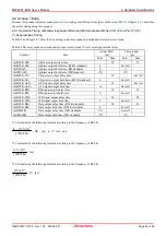
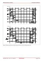
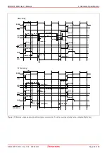
(2) Multiplex Bus Timing 

Table 4.3 and Figure 4.2 show the bus timing in memory expansion mode and microprocessor mode (2-wait, accessing 
external area, using multiplex bus). 
 
Table 4.3 Memory expansion mode and microprocessor mode (2-wait, accessing external area, using multiplex bus) 

Actual MCU 

[ns] 

This product 

[ns] 

Symbol Item 

Min. Max. Min. Max. 

td(BCLK-AD) 

Address output delay time 


50 


See left

th(BCLK-AD) 

Address output hold time (BCLK standard) 


See left 


th(RD-AD) 

Address output hold time (RD standard) 

(*1) 


(*4) 


th(WR-AD) 

Address output hold time (WR standard) 

(*1) 


(*4) 


td(BCLK-CS) 

Chip-select output delay time 


50 


See left

th(BCLK-CS) Chip-select 

output 

hold 

time (BCLK standard) 


See left 


th(RD-CS) 

Chip-select output hold time (RD standard) 

(*1) 


See left 


th(WR-CS) 

Chip-select output hold time (WR standard) 

(*1) 


See left 


td(BCLK-RD) 

RD signal output delay time 


40 


See left

th(BCLK-RD) 

RD signal output hold time 


See left 


td(BCLK-WR) 

WR signal output delay time 


40 


See left

th(BCLK-WR) 

WR signal output hold time 


See left 


td(BCLK-DB) 

Data output delay time (BCLK standard) 


50 


See left

th(BCLK-DB) 

Data output hold time (BCLK standard) 


See left 


td(DB-WR) 

Data output delay time (WR standard) 

(*2) 


See left 


th(WR-DB) 

Data output hold time (WR standard) 

(*1) 


See left 


td(BCLK-ALE) 

ALE output delay time (BCLK standard) 


40 


See left

th(BCLK-ALE) 

ALE output hold time (BCLK standard) 

-4 


See left 


td(AD-ALE) 

ALE output delay time (Address standard) 

(*3) 


See left 


th(ALE-AD) 

ALE output hold time (Address standard) 

(*4) 


See left 


td(AD-RD) 

After address RD signal output delay time 


-25 


td(AD-WR) 

After address WR signal output delay time 


-25 


tdz(RD-AD) Address 

output 

floating start time 


25 

 
*1 Calculated by the following formula according to the frequency of BCLK. 

)

(

10

5

.

0

9

BCLK

f

×

  [ns] 

 
*2 Calculated by the following formula according to the frequency of BCLK. 

(

)

50

)

(

10

5

.

0

9

×

BCLK

f

n

  [ns]  n: "2" for 2-wait 

 
*3 Calculated by the following formula according to the frequency of BCLK. 

40

)

(

10

5

.

0

9

×

BCLK

f

  [ns] 

 
*4 Calculated by the following formula according to the frequency of BCLK. 

15

)

(

10

5

.

0

9

×

BCLK

f

 [ns] 

Содержание Emulation Probe M306V8T-EPB

Страница 1: ...REJ10J0777 0100 T M306V8T EPB Rev 1 00 Aug 1 2005 User s Manual Emulation Probe for M16C 60 Series M16C 6V Group M306V8...

Страница 2: ...l inaccuracies or typographical errors Renesas Technology Corp assumes no responsibility for any damage liability or other loss rising from these inaccuracies or errors Please also pay attention to in...

Страница 3: ...Package components page 13 If there is any question or doubt about this product contact your local distributor The related manuals for using this product are listed below You can download the latest...

Страница 4: ...n your program development and evaluation stages In mass producing your program you have finished developing be sure to make a judgment on your own risk that it can be put to practical use by performi...

Страница 5: ...antly making efforts to improve the design and performance of this emulator Therefore the specification or design of this emulator or its user s manual may be changed without prior notice About the ri...

Страница 6: ...an imminently dangerous situation that will cause death or heavy wound unless it is avoided However there are no instances of such danger for the product presented in this user s manual WARNING WARNIN...

Страница 7: ...t a reliable ground connection is maintained If you smell a strange odor hear an unusual sound or see smoke coming from this product then disconnect power immediately by unplugging the AC power cable...

Страница 8: ...e communications interface cable or the flexible cable for connecting the user system And excessive flexing or force may break conductors Do not flex the flexible cable for connecting to the emulator...

Страница 9: ...01 23 2 5 Connecting the Power Supply for the Emulator 24 2 6 Turning ON the Power 25 2 6 1 Checking the Connections of the Emulator System 25 2 6 2 Turning ON OFF the Power 25 2 6 3 LED Display When...

Страница 10: ...Access Timing 65 4 2 1 Operation Timing of Memory Expansion Mode and Microprocessor Mode Vcc1 Vcc2 Vcc3 3 3V 65 4 3 Differences between the Actual MCU and Emulator 70 4 4 Connection Diagrams 73 4 5 Ex...

Страница 11: ...ill it in and FAX it to your local distributor or email the same contents to the following address Your registered information is used for only after sale services and not for any other purposes Witho...

Страница 12: ...nables debugging Firmware Program that analyzes contents of communication with the emulator debugger and controls the emulator hardware This program is installed in the flash memory in the emulator ma...

Страница 13: ...ircuit board 1 OSC 2 oscillator circuit bare board 1 Network registers for ports P0 P5 pullup 51k x 8 6 Hardware tool user registration FAX sheet English 1 Hardware tool user registration FAX sheet Ja...

Страница 14: ...6C 60 Series of the M16C 6V Group M306V8 MCUs the products listed below are necessary in addition to those contained package above Get them separately Table 1 2 Other tool products required for develo...

Страница 15: ...r connecting to 116 pin 0 65 mm pitch LQFP foot pattern on the user system For details refer to 2 9 Connecting the User System page 30 3 Emulator main unit PC7501 The emulator main unit for the M16C f...

Страница 16: ...ing ON Emulator system power supply is turned ON POWER OFF Emulator system power supply is turned OFF ON Emulator system is operating normally Flashing 1 The self check is being executed 2 Downloaded...

Страница 17: ...all the terminals Note on the Target Status CLOCK LED If the LED is not turned on check the following 1 After powering on the PC7501 before starting up the emulator debugger Make sure that the oscilla...

Страница 18: ...setting C variables run time execution Register reference setting Disassemble display C level debugging etc Real time trace function 256K cycle bus information recordable Bus external trigger time sta...

Страница 19: ...perating environment of the host machine Item Description Host machine IBM PC AT compatibles OS Windows Me Windows 98SE Windows XP Windows 2000 CPU Pentium III 600 MHz or more recommended Memory 128 M...

Страница 20: ...o the using interface Connect the M306V8T EPB to the emulator Connect the M306V8T EPB and the M3T FLX160 EPB of the PC7501 Connect the power supply for the emulator Connect a power supply for the emul...

Страница 21: ...e Renesas Debugger Package for M16C from the URL below http download renesas com eng mpumcu upgrades in_circuit_emulators m16c index html 2 Launching the installer Start the setup exe program 3 Enteri...

Страница 22: ...or PC7501 to a host machine you can choose your desired interface from LPT parallel interface USB interface and LAN interface Use the interface selection switch on the emulator PC7501 s rear panel to...

Страница 23: ...etal plate 6 Attach the metal plate 7 Tighten the two screws 8 Attach the upper cover 9 Slide the upper cover of the M306V8T EPB to the PC7501 side Figure 2 3 Connecting the PC7501 and emulation probe...

Страница 24: ...4 Connect the AC power cable to the receptacle CAUTION Cautions for AC Adapter Use only the AC adapter included in PC7501 package The included AC adapter is for PC7501 Do not use it for other product...

Страница 25: ...sly as possible Do not leave either the emulator or user system powered on because of leakage current the internal circuits may be damaged When turning ON the power again after shutting OFF the power...

Страница 26: ...s two or more Vcc terminals the LED does not light unless power is supplied to all the terminals Note on the Target Status CLOCK LED If the LED is not turned on check the following 1 After powering on...

Страница 27: ...ct the LPT parallel interface cable to the PC7501 and the host machine 2 Within 2 seconds of activating power to the emulator press the system reset switch on the PC7501 front panel to start maintenan...

Страница 28: ...shing POWER CLOCK RESET RUN WARNING POWER SAFE ERROR SYSTEM STATUS TARGET STATUS Maintenance mode started POWER CLOCK RESET RUN WARNING POWER SAFE ERROR SYSTEM STATUS TARGET STATUS Self check terminat...

Страница 29: ...OR 1 to ERROR 4 in Figure 2 6 check the following 1 Recheck the connection of the emulation probe and PC7501 2 Redownload the proper firmware IMPORTANT Note on the Self check Perform the self check wh...

Страница 30: ...product according to your user system Figure 2 7 Connecting the user system according to user systems CAUTION Note on Connecting the User System Take care not to attach a converter board in a wrong di...

Страница 31: ...Guide s 3 Connect M306V8T PTC to the YQPACK116SB Figure 2 8 Connecting to an 116 pin 0 65 mm pitch foot pattern NQPACK YQPACK YQSOCKET YQ GUIDE and HQPACK are trademarks of Tokyo Eletech Corporation...

Страница 32: ...gure 2 9 shows the positions of the switches of the M306V8T EPB Opening the upper cover 1 Slide aside the upper cover 2 Then pull the cover upward Closing the upper cover Attach the cover and slide it...

Страница 33: ...pF R9 1Mohm C12 0 1uF CNVSS2 A7 CVIN1 B4 VHOLD1 B3 HLF1 B2 CVIN2 A1 VHOLD2 C2 HLF2 D2 OSC1 OSCHLF L1 OSC2 VSYNC1 INT2 N3 VCC3 OSD C7 AN3 CAP C10 IC3 CVIN 1 R6 0ohm SW1 OSC1 R7 1kohm C13 2pF C14 0 015u...

Страница 34: ...cted use this setting JP2 VCC3 1 2 3 EPB TRGT Connects pin VCC3 of the evaluation MCU to the user system 1 2 3 EPB TRGT Factory setting Connects pin CNVSS2 of the evaluation MCU to GND in the M306V8T...

Страница 35: ...the internal circuit of the M306V8T EPB When the user system is not connected use this setting SW4 CVIN1 EPB TRGT SW4 CVIN1 Connects pin CVIN1 of the evaluation MCU to the user system EPB TRGT SW5 CVI...

Страница 36: ...edure 1 Pull the level 2 Pull the lever until it stops 3 Pull the evaluation MCU upward to remove it Evaluation MCU has been removed The data will be written into the OSDROM 4 Attach the evaluation MC...

Страница 37: ...3 lists the emulation port numbers and the pullup resistor part numbers Figure 2 12 Positions of the pullup resistors Table 2 3 Emulation ports and pullup resistor part numbers Port Resistor part P00...

Страница 38: ...nternal oscillator circuit 32 768 kHz Sub XCIN XCOUT External Oscillator circuit on the user system Yes IMPORTANT Notes on Changing the Clock Supply The clock supply can be set by the Init dialog box...

Страница 39: ...tup REJ10J0777 0100 Rev 1 00 2005 08 01 Page 39 of 90 2 Replacing an Oscillator Circuit Board 1 Remove the four screws of both sides of this product and lift off the upper cover see Figure 2 13 Figure...

Страница 40: ...tor circuit board Lift off the oscillator circuit board Attach another oscillator circuit board to the connector Secure the new oscillator circuit board with the screw Figure 2 14 Replacing the oscill...

Страница 41: ...ure 2 16 shows the circuitry of the oscillator circuit bare board OSC 2 Use the number of oscillator circuits recommended by the oscillator manufacturer Figure 2 15 External view of the oscillator cir...

Страница 42: ...ircuit in the PC7501 can generate any arbitrary frequency specified by the emulator debugger and it can be supplied as a main clock It does not depend on either the oscillator circuit board in the PC7...

Страница 43: ...the drop down list To connect to the PC7501 M16C Emulation Probe select SessionM16C_R8C_PC7501_Emulator 3 1 1 INIT Dialog Box After specifying the session an Init dialog box to connect the target is...

Страница 44: ...etup the following addresses are available 378h 278h Specifying the communication interface LAN communication For selecting the LAN communication click the radio button LAN of the MCU tab Specify the...

Страница 45: ...the address match break function Specify whether or not to use the address match break function To use the address match break function default Select the check box In this case the address match inte...

Страница 46: ...the load module user program size is small On Demand Debugging information is stored in a reusable temporary file on the hard disk of your computer Because the stored debugging information is reused...

Страница 47: ...file to be executed Clicking the Refer button brings up a file selection dialog box The script file you have selected is displayed in the Init File section of the dialog box shown here If you do not w...

Страница 48: ...al Mode Using or not using the internal reserved area expansion Specifies whether or not to expand the internal reserved area Check this box if the internal reserved area expansion bit PM13 is 1 PM13...

Страница 49: ...um operating frequency is 10MHz The box is unchecked by default 3 MCU Status Referring to the MCU Status It shows the status of each MCU pin Check it to see if the MCU status matches the selected proc...

Страница 50: ...MCU s internal flash ROM Specify whether or not you want the MCU s internal flash ROM to be cleared when downloading the user program or data When cleared the content of the flash ROM is initialized t...

Страница 51: ...3 Checking Connections of the Emulator System Checking connections of the emulator system When the emulator debugger is connected correctly to the emulator after you ve finished setting up the Init di...

Страница 52: ...he program up to the cursor position set or clear software breakpoints and line assemble the source file Because the present emulator uses the MCU s internal flash ROM the initial value for the ROM ar...

Страница 53: ...akpoints are set The address match break causes the program to stop before executing the address at which a breakpoint is set Software breakpoint A software breakpoint can be set or cleared by double...

Страница 54: ...05 08 01 Page 54 of 90 4 Executing up to the cursor position Come command 1 Specifying the Come command Setup procedure for executing COME command 1 Click the line in the program display area at which...

Страница 55: ...akpoint setup dialog box Hardware Break Point Clicking this button opens the hardware breakpoint setup dialog box 2 Hardware Break Point Setting Window in initial state H W breakpoint Setting Window i...

Страница 56: ...tects an instruction prefetch DATA ACCESS Detects a memory access BIT SYMBOL Detects a bit access INTERRUPT Detects an interrupt occurrence or interrupt termination TRIGGER Detects a signal from the e...

Страница 57: ...can set eight conditions e g a specified address a specified address range etc When you have finished setting the address click OK 2 Window for setting data Setting data You can set eight conditions e...

Страница 58: ...Data 1 00E5 MASK 00FF Access WRITE Setting events for wordwise accesses to the even addresses STE W A0 20E8h A0 5423h High order and low order data effective Setting events for wordwise accesses to th...

Страница 59: ...The program breaks when all of the specified events occur AND Same Time The program breaks when the specified events occur at the same time OR The program breaks when one of the specified events occur...

Страница 60: ...der of execution paths Disassemble data access mixed mode The executed instruction and the content of the accessed data can be inspected together Contents are displayed in order of the execution paths...

Страница 61: ...I O Symbol Status No change DMA Data access except for CPU INT Starts INTACK sequence IB Instruction code read bytes by CPU DB Data access bytes by CPU IW Instruction code read words by CPU DW Data a...

Страница 62: ...ce point condition was met is recorded Full 256K cycles of instruction execution after a trace began is recorded 2 Setting the trace write condition Setting the trace write condition You can specify a...

Страница 63: ...he blocks at the following addresses The background colors of the data display and the code display sections change with the access attribute as described below Green Addresses accessed for read Red A...

Страница 64: ...Applicable MCU M16C 60 Series M16C 6V Group M306V8 Evaluation MCU M306V8FJGS ROM size 512KB 4KB RAM size 16KB Applicable MCU mode Single chip mode Memory expansion mode 16 bit bus width NORMAL 4MB Mic...

Страница 65: ...ard 0 3 th WR AD Address output hold time WR standard 2 3 td BCLK CS Chip select output delay time 30 See left th BCLK CS Chip select output hold time BCLK standard 4 See left td BCLK ALE ALE signal o...

Страница 66: ...ad timing Write timing BCLK CSi ADi BHE ALE RD DBi td BCLK CS th BCLK CS tcyc td BCLK AD th BCLK AD th RD CS td BCLK ALE th BCLK ALE th RD AD td BCLK RD th BCLK RD tac2 RD DB Hi Z tsu DB RD th RD DB B...

Страница 67: ...gnal output hold time 0 See left td BCLK WR WR signal output delay time 40 See left th BCLK WR WR signal output hold time 0 See left td BCLK DB Data output delay time BCLK standard 50 See left th BCLK...

Страница 68: ...K CSi ADi BHE ALE RD ADi DBi td BCLK CS th BCLK CS tcyc td BCLK AD th BCLK AD th RD CS td BCLK ALE th BCLK ALE th RD AD td BCLK RD th BCLK RD tac3 RD DB Hi Z tsu DB RD th RD DB BCLK CSi ADi BHE ALE WR...

Страница 69: ...ta input hold time 0 See left th BCLK RDY RDY input hold time 0 See left th BCLK HOLD HOLD input hold time 0 See left td BCLK HLDA HLDA output delay time 40 See left Figure 4 3 Timing requirements Com...

Страница 70: ...those of actual MCU because there are a converter board and other devices between the evaluation MCU and the user system 7 Ports P0 to P5 P10 This product emulates some I O ports P0 to P5 P10 Therefor...

Страница 71: ...nterrupt stack pointer ISP is set to 00500h and used as stack area after the reset is released Notes on Maskable Interrupts Even if a user program is not being executed including when run time debuggi...

Страница 72: ...C2 bit PD9 address 0362h and 0366h registers cannot be done properly 1 Between when stop mode is released and when a hardware reset is executed 2 Between when low power dissipation mode is enabled and...

Страница 73: ...his product for reference purpose Figure 4 4 Connection diagram IC3 M16C 6V8 I O Emulate P67 P60 P77 P70 P83 P82 P91 P90 P86 Xcout P87 Xcin P86 Xcout P87 Xcin CNVss1 BYTE RESET Xin 74HC4066 74HC4066 5...

Страница 74: ...ff 12 0V 100 IIZ Leak current On output open 12 0V 100 A Table 4 6 Electrical characteristics of port emulation FPGA Standard values Symbol Item Condition Min Standard Max Unit VIH H level input volta...

Страница 75: ...0100 Rev 1 00 2005 08 01 Page 75 of 90 4 5 External Dimensions 4 5 1 External Dimensions of the Emulation Probe Figure 4 5 shows external dimensions of the M306V8T EPB Figure 4 5 External dimensions o...

Страница 76: ...ons of the M306V8T PTC Figure 4 6 shows external dimensions of the converter board M306V8T PTC for a 116 pin LCC included with the M306V8T EPB Figure 4 6 External dimensions of the M306V8T PTC 16 5 Un...

Страница 77: ...e product can be used by simply turning on the power Do not shut off the power while downloading the firmware If this happens the product will not start up properly If the power is shut off unexpected...

Страница 78: ...is product with a main clock XIN XOUT less than 1 MHz To use it with a main clock less than 1 MHz contact your local distributor Notes on Map Settings Be sure to set the OSDRAM area 8000h 8FFFh to INT...

Страница 79: ...ou reference the result of a trace in bus mode 00h is displayed The BRK instruction can be used for the emulator only You cannot use it in a user program You can neither set nor cancel a software brea...

Страница 80: ...n mode or microprocessor mode with this product the emulation memory can be allocated The emulation memory can be specified up to 4 areas by 4 MB in the MAP tab of the MCU setting dialog box of the em...

Страница 81: ...le the Address Match Interrupt Break Function in the MCU tab of the Init dialog box of the emulator debugger Thus normal software breaks are used for the internal RAM and ROM areas of an MCU Do not se...

Страница 82: ...ck the connection of power supply cable See 2 5 Connecting the Power Supply for the Emulator page24 2 Check that the power is properly supplied to the use system See 2 7 Downloading Firmware page27 3...

Страница 83: ...t See 2 4 Connecting the PC7501 page 23 Target Status POWER LED does not light up Connected Check that power Vcc is properly supplied to the user system and that the user system is properly grounded T...

Страница 84: ...Target MCU is in the reset state 1 Check the reset pin of the user system is pulled up 2 Check the reset pin of the user system has changed from L to H level Target MCU cannot be reset 1 In memory ex...

Страница 85: ...tup Table 5 3 Checkpoints of errors at debugger startup Error Checkpoint Target MCU is uncontrollable 1 Check that the NQPACK etc mounted on the user system is soldered properly 2 Check that the conne...

Страница 86: ...1U PC4701M PC4701HS PC4701L PC7501 Other 3 Emulator s serial number 4 Product name of the emulation pod probe 5 Serial number of the emulation pod probe 6 Interface USB LPT parallels LAN Serial Dedica...

Страница 87: ...f the following causes we will repair it or replace it with new one with extra charge Misuse abuse or use under extraordinary conditions Unauthorized repair remodeling maintenance and so on Inadequate...

Страница 88: ...equest Sheet is written in as much detail as possible to facilitate repair Distributor After checking the contents of fault the distributor should please send the faulty product along with the Repair...

Страница 89: ...T EPB Publication Date Aug 1 2005 Rev 1 00 Published by Sales Strategic Planning Div Renesas Technology Corp Edited by Microcomputer Tool Development Department Renesas Solutions Corp 2005 Renesas Tec...

Страница 90: ...M306V8T EPB User s Manual...

Отзывы: