Smart Wi-Fi Module Series
SC20-WL Hardware Design
SC20-WL_Hardware_Design
54 / 81
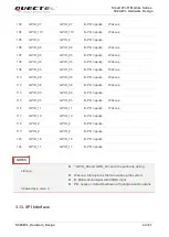
The following is a reference circuit design for front camera interface, by taking the connection with
SP2508 camera as an example.
MIPI_CSI1_CLKP
DGND
DGND
CLKP
CLKN
DGND
MDN0
DGND
MCLK
CAM_I2C_SDA
100nF
CAM_I2C_SCL
CAM1_RST
MIPI_CSI1_CLKN
MIPI_CSI1_LN0P
MIPI_CSI1_LN0N
CAM1_PWD
CAM1_MCLK
DGND
MDP0
DGND
DGND
NC(MDP1)
NC(MDN1)
DGND
DGND
SCL
SDA
PWDN
RST
AVDD2V8
AGND
DGND
DOVDD1V8
NC
1uF
2.2uF
0R
LDO17_2V85
LDO6_1V8
1
2
3
4
5
6
7
8
9
10
11
12
13
14
15
16
17
18
19
20
21
22
23
24
25
100nF
2.2K
2.2K
1
2
3
4
5
6
1
2
3
4
5
6
LDO6_1V8
Module
Front Camera
FL2
FL1
R2
R1
R3
C1
C2
C3
C4
EMI Filter
Figure 23: Reference Circuit Design for Front Camera Interface
I
O
max=100mA
LDO17_2V85
129
PO
2.85V output power supply
for AVDD of camera
2.85V normal voltage.
Vnorm=2.85V
I
O
max=300mA
MIPI_CSI1_CLKN
70
AI
MIPI CSI clock signal
(negative)
MIPI_CSI1_CLKP
71
AI
MIPI CSI clock signal
(positive)
MIPI_CSI1_LN0N
72
AI
MIPI CSI data signal
(negative)
MIPI_CSI1_LN0P
73
AI
MIPI CSI data signal
(positive)
CAM1_MCLK
75
DO
Clock signal of front camera
CAM1_RST
81
DO
Reset signal of front camera
CAM1_PWD
82
DO
Power down signal of front
camera
CAM_I2C_SCL
83
OD
I2C clock signal of camera
CAM_I2C_SDA
84
OD
I2C data signal of camera


