PDP-503PE, PDP-503PU
92
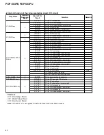
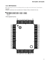
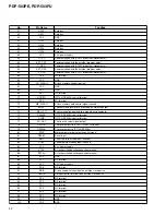
No.
Pin Name
Function
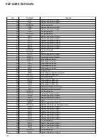
51
UD10
Data bus
52
UD11
Data bus
53
VSS
GND
54
UD12
Data bus
55
UD13
Data bus
56
UD14
Data bus
57
UD15
Data bus
58
VCC
3.3V power supply
59
D_TXD
Communication with IC1207 (module microcomputer)
60
EXT_TXD
Communication with the outside (program notes)
61
D_RXD
Communication with IC1207 (module microcomputer)
62
EXT_RXD
Communication with the outside (program notes)
63
D_CLK
Communication with IC1207 (module microcomputer)
64
P60
NC terminal
65
VSS
GND
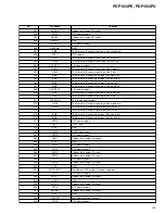
66
CS_FLASH
A flash memory control terminal
67
VSS
GND
68
VSS
GND
69
P61
NC terminal
70
UDREQ
IC1703 (PE5064) control terminal
71
P63
NC terminal
72
WE_FLASH
A flash memory note control signal (unused)
73
BUSY
The command receipt of a message lye Norwich output
74
REQ_PU
A communication demand to a module microcomputer
75
SEL23B
IC1703 (PE5064) control terminal
76
CLRB
IC1703 (PE5064) control terminal
77
FR_SEL
The free run select signal output
78
RST31B
The reset output to IC1301, IC1401 (PD6358)
79
RST23B
The reset output to IC1703 (PE5064)
80
FWE
Microcomputer program note control signal
81
RESET
Reset input
82
NMI
The at the rate of tang input (unused)
83
STBY
The hardware standby input (unused)
84
VCC
3.3V power supply
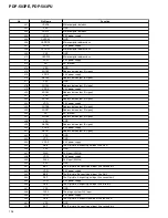
85
XTAL
A clock oscillation child connection terminal
86
EXTAL
A clock oscillation child connection terminal
87
VSS
GND
88
PF7
NC terminal
89
VCC
3.3V power supply
90
PF6
NC terminal
91
RDB
A read control terminal from an outside slave device
92
HWRB
A wright control terminal to an outside slave device
93
PF3
NC terminal
94
PF2
NC terminal
95
PF1
NC terminal
96
PF0
NC terminal
97
P50
NC terminal
98
P51
NC terminal
99
VSS
GND
100
VSS
GND

