110
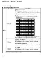
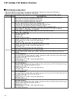
PDP-503CMX, PDP-503MXE, PDA-5002
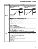
Use this sustain pulse
and adjust.
Magnify 6SF block
Magnify the adjustment waveform
Magnify 6SF block
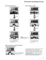
CH1 : Y SUSOUT Under (K2203), 50V/div
CH2 : Y SUSOUT Upper (K2212), 50V/div
CH4 : YPR-U1 (K2038)- Trigger, 5V/div
Trigger : 2msec delay
CH1 : Y SUSOUT Under (K2203), 50V/div
CH2 : Y SUSOUT Upper (K2212), 50V/div
CH4 : YPR-U1 (K2038)- Trigger, 5V/div
Trigger : 2msec delay
CH1 : X SUSOUT Under (K3106), 50V/div
CH2 : X SUSOUT Upper (K3105), 50V/div
CH4 : YPR-U1 (K2038)- Trigger, 5V/div
Trigger : 2msec delay
Y DRIVE SUSOUT waveform
X DRIVE SUSOUT waveform
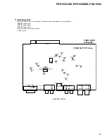
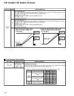
Measuring point of waveform
Waveform coarse adjustment
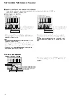
Measuring Waveform of Pulse Module Timing Adjustment
Timing adjustment of the pulse module control signal adjusts with the sustain pulse of eighth pulse (X DRIVE) and
the ninth pulse (Y DRIVE) from the back of 6SF.
Measure the SUSOUT waveform
1SF
2SF 3SF 4SF 5SF 6SF 7SF
1ms/div
5
µ
s/div
1SF
2SF 3SF 4SF 5SF 6SF 7SF
1ms/div
5
µ
s/div
• Perform adjustment of waveform with a black mask screen.
• It is easy to adjust when turned field AB offset to OFF (RS-232C
command: OCN) in adjustment.
Note:
• Sampling rate of oscilloscope sets it more than 500MS/s in order
to perform ns order adjustment.
• Collecting calibration of probe before adjustment by all means.
• Connect GND of probe measuring waveform to SUSGND terminal
by all means.
• Precise waveform is not displayed, and an adjustment gap may
occur that does not collect GND properly.
When took waveform be each drive Assy unit, measure it at the
fourth sustain pulse from the back except for a large width sustain
pulse.
Therefore, when measured both waveform of the X and Y drives
together, it becomes the sustain pulse of 8 and 9 pulses from the
back.
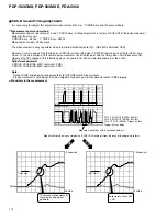
When there is a gap with waveform of CH1 / CH2 of the part which
enclosed in the following circle, adjust required VR to overlap the
waveform.
Adjust with SUS-B
Adjust with SUS-U
Adjust with SUS-G
1ms/div
500ns/div
Use this sustain pulse
and adjust.
Содержание PDA-5002
Страница 5: ...5 PDP 503CMX PDP 503MXE PDA 5002 ...
Страница 143: ...PDP 503CMX PDP 503MXE PDA 5002 143 Block Diagram Pin Function ...
Страница 166: ...PDP 503CMX PDP 503MXE PDA 5002 166 Pin Assignment Top View CXA3516R RGB ASSY IC4603 AD PLL IC ...
Страница 167: ...PDP 503CMX PDP 503MXE PDA 5002 167 Block Diagram ...
Страница 168: ...PDP 503CMX PDP 503MXE PDA 5002 168 Pin Function ...
Страница 169: ...PDP 503CMX PDP 503MXE PDA 5002 169 ...
Страница 170: ...PDP 503CMX PDP 503MXE PDA 5002 170 ...

