104
PDP-503CMX, PDP-503MXE, PDA-5002
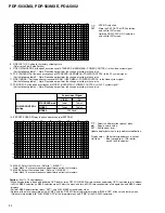
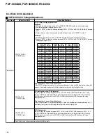
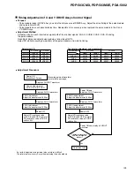
VOFS (Offset voltage) adjustment
Method 1
1. Write down a adjustment value of V-OFFSET of REF-DIG mode in the factory mode.
2. Set this adjustment value to center (128).
3. Adjust VR2701 so that the voltage between K2701 (VOFS) and K2703 (SUS GND) becomes
45V.
4. Return it to the value that wrote down a adjustment value of V-OFFSET in step 1.
Method 2
1. Read the adjustment value of V-OFFSET of REF-DIG mode in the factory mode.
2. Adjust VR2701 so that the voltage between K2710 (VOFS) and K2703 (SUS GND) becomes
following voltage
±
0.5V.
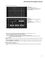
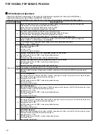
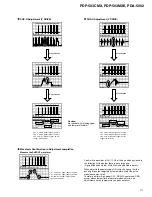
VH (voltage for scan IC) Adjustment
Adjust so that the voltage between K2716 (VH) and K2720 (PSUS) becomes 103V
±
0.5V.
PSUS (=GNDH) is a floating GND and the electric potential is different from that of chassis
GND. Be sure not to short-circuit PSUS (=GNDH) and another GND, because that may
damage the unit.
The symptom is case of mis-adjustment
If the VH adjustment is not performed properly, dots like blinking luminance points appear. If
deviated greatly from the right adjustment point, panel will light white.
Input Signal
Adjusting Point
Adjusting Method
White 100%
VR2701 (VOFS)
(Y DRIVE Assy)
VR2703 (VH)
(Y DRIVE Assy)
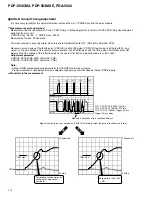
IC5V Adjustment
Adjust so that the voltage between K2707 (IC5V) and K2720 (PSUS) becomes 5.0V
±
0.1V.
PSUS (=GNDH) is a floating GND and the electric potential is different from that of chassis
GND. Be sure not to short-circuit PSUS (=GNDH) and another GND, because that may
damage the unit.
The symptom is case of mis-adjustment
If the VOFS Voltage adjustment is not performed properly, dots like blinking luminance points
appear. If deviated greatly from the right adjustment point, panel will light white.
VR2702 (IC5V)
(Y DRIVE Assy)
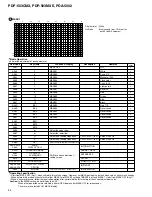
Note : Be sure to measure between specified test points.
Input
Command
DAC
Output
Setting
Voltage
Input
Command
DAC
Output
Setting
Voltage
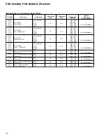
VOF000
0.4
25
VOF134
2.599212598
45.94488
VOF006
0.4984375
25.9375
VOF141
2.71496063
47.04724
VOF013
0.61328125
27.03125
VOF147
2.814173228
47.99213
VOF019
0.71171875
27.96875
VOF153
2.913385827
48.93701
VOF026
0.8265625
29.0625
VOF160
3.029133858
50.03937
VOF032
0.925
30
VOF166
3.128346457
50.98425
VOF038
1.0234375
30.9375
VOF172
3.227559055
51.92913
VOF045
1.13828125
32.03125
VOF179
3.343307087
53.0315
VOF051
1.23671875
32.96875
VOF185
3.442519685
53.97638
VOF058
1.3515625
34.0625
VOF191
3.541732283
54.92126
VOF064
1.45
35
VOF198
3.657480315
56.02362
VOF070
1.5484375
35.9375
VOF204
3.756692913
56.9685
VOF077
1.66328125
37.03125
VOF211
3.872440945
58.07087
VOF083
1.76171875
37.96875
VOF217
3.971653543
59.01575
VOF090
1.8765625
39.0625
VOF223
4.070866142
59.96063
VOF096
1.975
40
VOF230
4.186614173
61.06299
VOF102
2.0734375
40.9375
VOF236
4.285826772
62.00787
VOF109
2.18828125
42.03125
VOF242
4.38503937
62.95276
VOF115
2.28671875
42.96875
VOF249
4.500787402
64.05512
VOF122
2.4015625
44.0625
VOF255
4.6
65
VOF128
2.5
45
6.3.2 Main Unit Adjustment
VOFS/VH/IC5V Voltage Adjustment
Содержание PDA-5002
Страница 5: ...5 PDP 503CMX PDP 503MXE PDA 5002 ...
Страница 143: ...PDP 503CMX PDP 503MXE PDA 5002 143 Block Diagram Pin Function ...
Страница 166: ...PDP 503CMX PDP 503MXE PDA 5002 166 Pin Assignment Top View CXA3516R RGB ASSY IC4603 AD PLL IC ...
Страница 167: ...PDP 503CMX PDP 503MXE PDA 5002 167 Block Diagram ...
Страница 168: ...PDP 503CMX PDP 503MXE PDA 5002 168 Pin Function ...
Страница 169: ...PDP 503CMX PDP 503MXE PDA 5002 169 ...
Страница 170: ...PDP 503CMX PDP 503MXE PDA 5002 170 ...


