3
CX-890
2. CIRCUIT DESCRIPTIONS
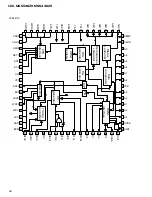
2.1 Preamplifier (UPC2572GS: IC101)
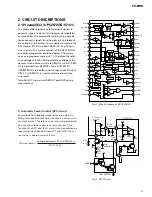
The preamplifier processes pickup output signals to
generate signals to be sent to the servo, demodulator,
and controller. The preamplifier with built-in photode-
tector converts signals from the pickup into intermedi-
ate voltage in the pickup. Then, addition is made in the
RF amplifier (IC101) to obtain RF, FE, TE, and TE zero
cross signals. The system consists of the UPC2572GS
and other components explained below. The system
uses a single power source (+5 V). Therefore, the refer-
ence voltage of IC101 and the reference voltage of the
power unit and servo circuit are REFOUT (+2.5 V). REFO
UT is obtained from REFOUT of servo LSI (IC201:
UPD63702GF) via a buffer, and is output from Pin 19 of
IC101. This REFOUT is used as reference for all mea-
surements.
Note:Do NOT short-circuit REFOUT and GND during
measurement.
1
2
3
4
5
6
7
8
9
10
11
12
13
14
15
16
17
18
19
38
37
36
35
34
33
32
31
30
29
28
27
26
25
24
23
22
21
20
X12
RF
envelope
AGC
Detection
X3
Phase detection
3T detection
Bottom
DC shift
Peak
Control
DC shift
Bottom
Peak
120k
Ω
DEFECT circuit
FE BAL
FE
BAL
Vcc
Mirror circuit
FE BAL
APC
X2
Vcc
FE-BAL
TE-BAL
ASY
EFM-OUT
C.DEF
DEFECT
RFOK
MIRR
3T-OUT
C.FE
FE-OUT
FE-
GND
TE-
TE-OUT1
TE-OUT2
DET-IN
DET-OUT
VREF-IN
VREF-OUT
LDON
LD
PD
E
F
D
B
C
A
Vcc
C2.3T
C1.3T
RF-
RF-OUT
RF-IN
C AGC
AGC-OUT
EFM-IN
HPF
TE
BAL
EFM comparator
Control
Fig. 1 Block Diagram of UPC2572GS
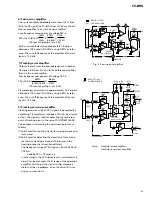
1) Automatic Power Control (APC) circuit
Laser diode has negative temperature characteristics
with great optical output when the diode is driven with
constant current. Therefore, current must be controlled
by a monitor diode to ensure constant output. Thus
functions the APC circuit. LD current can be obtained by
measuring the voltage between LD1 and GND. The cur-
rent value is approximately 35 mA.
Vcc (5V)
Vr
LD
MD
UPC2572GS
16
PD
17
LD
15
Q101
2SD1664
C124
0.1
µ
F
C101
(100
µ
F/6.3V)
R101
10
Ω
LD1
R102
12
Ω
5V
CONT
Q102 UMD2N
18
5V
5V
1k
Ω
150k
Ω
16k
Ω
R112
2.2k
Ω
C104
0.33
µ
F
5
1k
Ω
2.5V
Pickup unit
Fig. 2 APC Circuit
Voltage between LD1 and GND(mv)
LD current(mA) =
10
Ω
+ 12
Ω
Содержание CDX-MG6056ZH
Страница 5: ...4 CDX MG6346ZH MG6446ZH 2 2 EXTERIOR ...
Страница 7: ...6 CDX MG6346ZH MG6446ZH 2 3 CD MECHANISM ...
Страница 14: ...13 CDX MG6346ZH MG6446ZH 5 6 7 8 5 6 7 8 D C B A A A b A EXTENSION UNIT ...
Страница 15: ...14 CDX MG6346ZH MG6446ZH 1 2 3 4 1 2 3 4 D C B A 1 A a A b D CD CORE UNIT STS UNIT A a ...
Страница 16: ...15 CDX MG6346ZH MG6446ZH 5 6 7 8 5 6 7 8 D C B A A a A b B 2 B KEYBOARD UNIT A a ...
Страница 17: ...16 CDX MG6346ZH MG6446ZH 1 2 3 4 1 2 3 4 D C B A A a A b 1 A EXTENSION UNIT A b ...
Страница 18: ...17 CDX MG6346ZH MG6446ZH 5 6 7 8 5 6 7 8 D C B A A a A b 2 A b ...
Страница 28: ...27 CDX MG6346ZH MG6446ZH 1 2 3 4 1 2 3 4 D C B A CN701 CN901 EXTENSION UNIT SIDE B A A B D ...
Страница 29: ...28 CDX MG6346ZH MG6446ZH 1 2 3 4 1 2 3 4 D C B A 4 2 KEYBOARD UNIT KEYBOARD UNIT CN701 SIDE A B B A ...
Страница 30: ...29 CDX MG6346ZH MG6446ZH 1 2 3 4 1 2 3 4 D C B A SIDE B KEYBOARD UNIT B B ...
Страница 32: ...31 CDX MG6346ZH MG6446ZH 1 2 3 4 1 2 3 4 D C B A CD CORE UNIT SERVO UNIT SIDE B C C ...
Страница 34: ...33 CDX MG6346ZH MG6446ZH 1 2 3 4 1 2 3 4 D C B A CD CORE UNIT STS UNIT SIDE B D D ...
Страница 35: ...34 CDX MG6346ZH MG6446ZH 1 2 3 4 1 2 3 4 D C B A 4 5 MOTOR PCB B MOTOR PCB B E E SPINDLE MOTOR M5 ...
Страница 36: ...M M4 CARRIAGE 1 12 D CN301 35 CDX MG6346ZH MG6446ZH 5 6 7 8 5 6 7 8 D C B A E C ...
Страница 38: ...1 41 G CN801 37 CDX MG6346ZH MG6446ZH 1 2 3 4 1 2 3 4 D C B A MOTOR PCB A F SIDE B F D ...
Страница 40: ...39 CDX MG6346ZH MG6446ZH 1 2 3 4 1 2 3 4 D C B A 4 9 PCB UNIT E PCB UNIT E PCB UNIT E SIDE A SIDE B I I I ...
Страница 48: ...47 CDX MG6346ZH MG6446ZH Grating waveform Ech Xch 20mV div AC Fch Ych 20mV div AC 45 0 75 60 30 90 ...

