7.
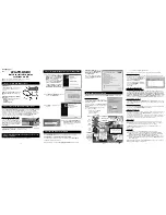
Circuit Diagrams and PWB Layouts
TV & Scaler Board: HDMI
4X1
G4
4X2
1
2
VDD
VEE VSS
DIGITAL
DE-EMPHASIS
INTERPOLATION
DAC
NOISE SHAPER
FILTER
INTERFACE
DAC
SCL
ADR
0
1
2
SDA
WC
22
21
20
19
18
17
16
15
14
13
12
11
10
9
8
7
6
5
RSET
RX2+
RX2-
RX1+
RX1-
RESET
MCLKIN
CSCL
CSDA
DSCL
DSDA
RXC-
VSYNC
GND
PGND
OGND
RSVDL
DE
ODCK
INT
Q
NC
RXC+
RX0-
RX0+
AGND
GND_HS
DACGNDG
DACGNDB
DACGND
DACGNDR
23
VCC
AVCC
MCLKOUT
OVCC1
DACVCCB
DACVCCG
DACVCCR
DACVCC
PVCC2
PVCC1
ANRPR
ANGY
ANBPB
SPDIF
SDO
WS
SCK
HSYNC
4
3
2
1
0
RSVDO
EXT-RES
PLLOUT
PLLIN
COMP
NC
NC
NC
NC
91R
HDMI
(RESERVE)
TO 1690 OF IO BOARD
(HDMI CONNECTOR)
NC
NC
NC
(RESERVE)
NC
AUDIO DAC
A7
A7
A11
(MAINLY FOR NAFTA)
FOR NON HDMI SET
3V3
3V3
3V3
3V3
3V3
0V
0V
0V
0V
0V
2V8
3V2
3V3
2V1
1V6
3V3
1V6
0V
0V
1V7
0V
1V7
1V7
0V
1
2
3
4
5
6
7
8
9
10
11
12
13
14
15
1
2
3
4
5
6
7
8
9
10
11
12
13
14
15
A
B
C
D
E
F
G
H
1801 E1
2803 A5
2804 F14
2805 G14
2806 A8
2807 A5
2808 A8
2809 A7
2810 A5
2811 B5
2812 B3
2813 A6
2814 A7
2815 B8
2816 A5
2817 B5
2818 A6
2819 A6
2820 B7
2821 B8
2822 B5
2823 B5
2824 A6
2825 B6
2826 B7
2827 B8
2828 B5
2829 B5
2830 B6
2832 D2
2833 E11
2834 E12
2835 E11
2836 E12
2837 F3
2838 F3
2839 F3
2840 F3
2841 G11
2842 G13
2843 G12
2844 G12
2845 G11
2846 G13
2847 E13
2848 E13
2849 G2
3801-1 A11
3801-2 A11
3801-3 A11
3801-4 A11
3802-1 B11
3802-2 B11
3802-3 B11
3802-4 B11
3803-1 B11
3803-2 B11
3803-3 B11
3803-4 C11
3804-1 C11
3804-2 C11
3804-3 C11
3804-4 C11
3805-1 C11
3805-2 C11
3805-3 D11
3805-4 D11
3806-1 D11
3806-2 D11
3806-3 D11
3806-4 D11
3807 G9
3808 B2
3809 B2
3810 B2
3813-1 G9
3813-2 F9
3813-3 F9
3813-4 F9
3815 G11
3816 G11
3817 G12
3819 G12
3821 C4
3822 C4
3823 C4
3824 C3
3825 C3
3826 E12
3827 E12
3829 F14
3830 G9
3831 F4
3833 F14
3834 F4
3835 B5
3836 E14
3837 G14
3838 E14
3839 G14
4836 F15
4838 F15
5801 A5
5802 A5
5803 A7
5804 A6
5805 A6
7801 B1
7806 D3
7807 D3
7808 C5
7809 E11
7810 F13
F801 A6
F802 A5
F803 A7
F804 A6
F805 A6
F806 H2
F807 H2
F808 H6
F809 B2
F810 F10
F811 E14
F812 F2
F813 F2
F814 F2
F815 F2
F816 F2
F817 F2
F818 F2
F819 F2
F820 G2
F821 G2
F822 G2
F823 G2
F824 G1
F826 E11
F827 E12
F828 F10
F829 F10
F830 G10
I802 D2
I803 D2
I810 F9
I811 G12
I812 F4
I813 F4
I814 F4
I815 G11
I816 G11
I817 C5
I818 D4
I819 G13
I822 D4
I829 F14
I833 G14
I834 F4
I836 E13
I838 E13
I840 F4
I841 G11
I842 G12
I844 G12
I847 E13
I848 E13
FOR ALL SET
2805
1u0
2804
1u0
I833
I829
F830
F829
I818
F828
I817
I813
I814
I812
I810
I811
F823
F824
F822
F820
F821
F818
F819
F816
F817
F815
F814
F812
F813
F811
F826
F827
F810
F807
F808
F806
F805
F803
F801
F804
F802
4838
F809
4836
I834
I840
I822
I802
I803
I816
I841
I815
I819
I844
I842
I847
I848
I838
I836
+3V3STBY
+5VHDMI
3833
3829
10K
10K
2849
10n
2848
1u0
1u0
2847
3837
10K
10K
3836
3839
10K
3838
10K
3
4
5
6
7
8
9
21
22
12
13
14
15
16
17
18
19
2
20
1801
1
10
11
390R
3835
+3V3STBY
3834
13
1
3
14
15
4
11
10
9
16
7
8
12
2
5
MDX
7810
HEF4053B
6
3807
33R
33R
33R
4
5
3830
33R
3
6
3806-4
2
7
3806-3
1
8
3806-2
33R
4
5
3806-1
33R
33R
3805-4
33R
3805-3 3
6
3805-2
33R
2
7
33R
1
8
4
5
3805-1
3
6
33R
3804-4
7
33R
3804-3
8
3804-2
33R
2
3804-1
33R
1
33R
3803-4 4
5
33R
3803-3 3
6
33R
3803-2 2
7
3803-1 1
8
4
5
33R
3
6
33R
3802-4
7
33R
3802-3
8
33R
3802-2 2
3802-1
33R
1
100n
2846
3819
100R
3817
220K
10V
2842
1u0
100n
2845
100R
3815
220K
3816
1u0 10V
2841
2843
6.3V
2844
47u
1R0
100n
3826
3827
1R0
6.3V
47u
2834
100n
2836
+3V3STBY
47u 6.3V
2833
100n
2835
5 33R
3801-4 4
33R
3801-3 3
6
33R
3801-2 2
7
33R
1
8
16
VREF-DAC
12
VSSA
15
VSSD
5
WS
2
3801-1
PCS
10
SFOR0
11
SFOR1
7
SYSCLK
6
VDDA
13
VDDD
4
VOL
14
VOR
UDA1334BT/N2
7809
BCK
1
DATAI
3
DEEM
9
MUTE
8
6.3V
2806
22u
1n0
2815
2820
1n0
1n0
2822
1n0
2811
5801
5
3813-4
33R
4
33R
3813-3 3
6
33R
3813-2 2
7
33R
3813-1 1
8
3K9
3831
10u
2840
10n
2838
47n
2839
10u
2837
2832
1n0
100n
2812
3810
4K7
3809
4K7
4K7
3808
2
3
6
5
8
4
7
M24C02-WMN6
EEPROM
(256x8)
7801
1
+3V3STBY
+3V3STBY
+3V3STBY
+3V3STBY
4K7
3822
4K7
3823
3824
3825
100R
7806
100R
BSN20
BSN20
7807
3821
33R
5802
+3V3STBY
+3V3STBY
+3V3STBY
5804
2818
16V 10u
16V
2813
10u
5805
5803
+3V3STBY
22u
+3V3STBY
2809
6.3V
2803
6.3V
22u
2810
6.3V
22u
2808
100n
2814
100n
2819
100n
2824
100n
2807
100n
100n
2816
1n0
2821
1n0
2827
1n0
2826
1n0
2825
1n0
2830
1n0
2817
1n0
2823
1n0
2829
2828
100
34
31
1n0
91
97
96
84
83
32
30
29
17
40
64
55
72
9
18
73
19
20
87
86
92
68
39
38
37
36
63
62
61
60
59
58
54
53
52
51
50
49
48
44
43
42
56
67
79
22
24
25
80
23
70
69
26
3
4
46
28
45
57
66
78
21
47
76
81
16
41
65
99
101
33
71
27
2
13
10
5
1
14
11
6
35
77
98
15
12
7
82
89
93
95
8
74
75
HDMI
PANELLINK
RECEIVER
SII9993CT100
7808
85
88
90
94
CEC
PC_AUDIO_R
PC_AUDIO_L
HDMI_VBLU4
HDMI_VBLU5
HDMI_VBLU6
HDMI_VBLU7
HDMI_VGRN0
HDMI_VGRN1
HDMI_VGRN2
HDMI_VGRN3
HDMI_VGRN4
HDMI_VGRN5
HDMI_VGRN6
HDMI_VGRN7
HDMI_VRED0
HDMI_VRED1
HDMI_VRED2
HDMI_VRED3
HDMI_VRED4
HDMI_VRED5
HDMI_VRED6
HDMI_VRED7
HDMI_VDV
HDMI_VCLK
PC_HDMI-AUDIO_SEL
AudioIN2L
AudioIN2R
DOC_SCL
HDMI_VBLU0
HDMI_VBLU1
HDMI_VBLU2
HDMI_VBLU3
RXC+
RXC-
SPDIF
HDMI_VVS
SCL_IO
SDA_IO
DOC_SDA
COMP
COMP
HDMI_VHS
PLLIN
PLLIN
#RESET
RX0+
RX0-
RX1+
RX1-
RX2+
RX2-
E_14490_036.eps
190404
3139 123 5804.2
Содержание LC4.2HE
Страница 18: ...Service Modes Error Codes and Fault Finding EN 18 LC4 2HE AA 5 Personal Notes E_06532_012 eps 131004 ...
Страница 58: ...58 LC4 2HE AA 7 Circuit Diagrams and PWB Layouts Personal Notes ...
Страница 78: ...Revision List EN 78 LC4 2HE AA 11 11 Revision List Manual xxxx xxx xxxx 0 First release ...