EN 53
HTS5000W
9.
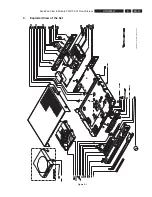
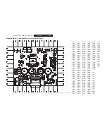
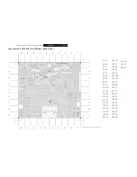
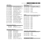
Exploded View & Module PWR 04-01 Non-Wireless
4.
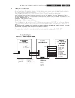
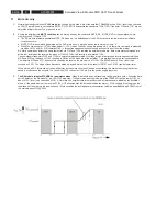
** Disconnecting the surround ampli
fi
er from the mains results in the following: A fast mutecommand is produced by the circuitry around
7103. This helps assuring plopfree operation. At the same moment 7131 saturates and enables an extra load of 47 ohm on the 6Vdc
line: result is s a clean drop-down of the 6Vdc line. Out of the pulse on the base of 7131, 7108 and C 2194 produce a clean powerdown
signal. This powerdown pulse is used by the receiver to start up a powerdown sequence and an additional fast mute on the audiolines
of the RX-board. All these additional circuitry assures absolute plop- and glitch free operation in any circumstance.
5.
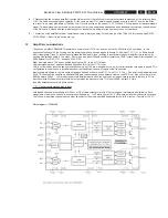
** At start up of the ampli
fi
er-receiver combination: there is always a delay on the mode pin of the TDA8920, this is done with R3125 /
C2185 (100
μ
F). Result is a plop-free startup.
12 Ampli
fi
er considerations
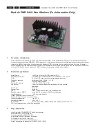
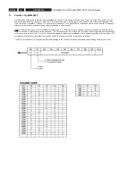
The chosen ampli
fi
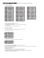
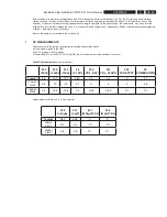
er TDA8920BTH operates on symme/-27.5 Vdc and can deliver 2 x 50 Watts into 6 ohm loads. In this
application the heat sink, the housing and the power supply have been designed to assure 2 x 50 watts FTC (***) or 2 x 50 watts with
music-like signals. Class D - technology minimizes the dissipation, thus resulting in an ef
fi
cient high power ampli
fi
er in a rather small
housing with limited heatsink. The class - D chip runs on a about 300kHz oscillator, therefore a 12dB / octave output
fi
lter is needed for
EMI approval (coil 5100, 5101, and caps 2154, 2155)
Right input signals are 180° phase shifted by using the IN1 - (pin 9of 7110) input.
Left input signals are not phase shifted and applied on IN2 +(pin5 of 7110) input.
This is not a problem since the speaker connections in plug 1100 are managed in such a way that left and right are again in phase. This
con
fi
guration is used to have a good balanced current handling of the power supply at low frequencies.
Input signals are
fi
ltered in the two-section high pass Sallen Key
fi
lter around 7111-1 and 7111-2. The – 3 db point is somewhere around
30Hz. This
fi
lter section has also an additional 6dB gain to assure good sound balance with the used DVD set. Also notice that a lot of
EMI capacitors (100pF – 1nF) are designed in this ampli
fi
er board, since the
fi
nal unit has to pass severe immunity tests up to 2 GHz.
Input sensitivity of the ampli
fi
er for maximum output when the attenuator chip 7113 is set to 0dB: typical 0.5 Vrms.
(see also datasheets concerning this device).
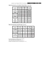
*** FTC power considerations & de
fi
nitions.
both loaded channels are preheated for 1 hour at 1/8 of rated output power with a 1kHz sinewave. Immediately after follows a 5-min
measurement where one channel is driven at speci
fi
ed power (= 50 watts @ max 10% THD) whereas the other channel is not driven.
The full power operated channel has to deliver its power for the whole-speci
fi
ed bandwidth for the full 5 minutes. (T-ambient = 25°C).
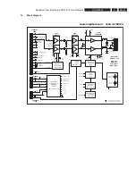
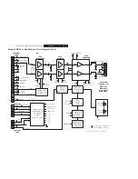
Blockdiagram
of
TDA8920B
Содержание HTS5000W/12
Страница 15: ...EN 15 HTS5000W FTD Display Pin Connection 6 6 FTD Display Pin Connection ...
Страница 16: ...EN 16 HTS5000W Notes 6 FTD Display Pin Connection ...
Страница 40: ...EN 40 HTS5000W Notes Circuit Diagram and PWB Layout 8 ...
Страница 60: ...EN 60 HTS5000W 9 Exploded View Module PWR 04 01 Non Wireless Notes ...

