


5-5
5-5
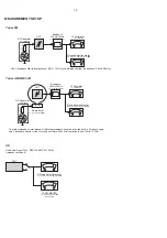
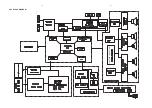
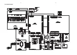
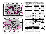
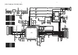
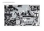
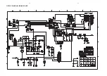
PCB LAYOUT - KEY BOARD
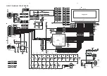
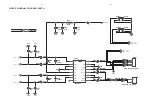
2. 380V
3. 151V
2. 979V
2. 709V
2. 108V
R247
47K
R247
47K
R246
20K
R246
20K
R256
8K2
R256
8K2
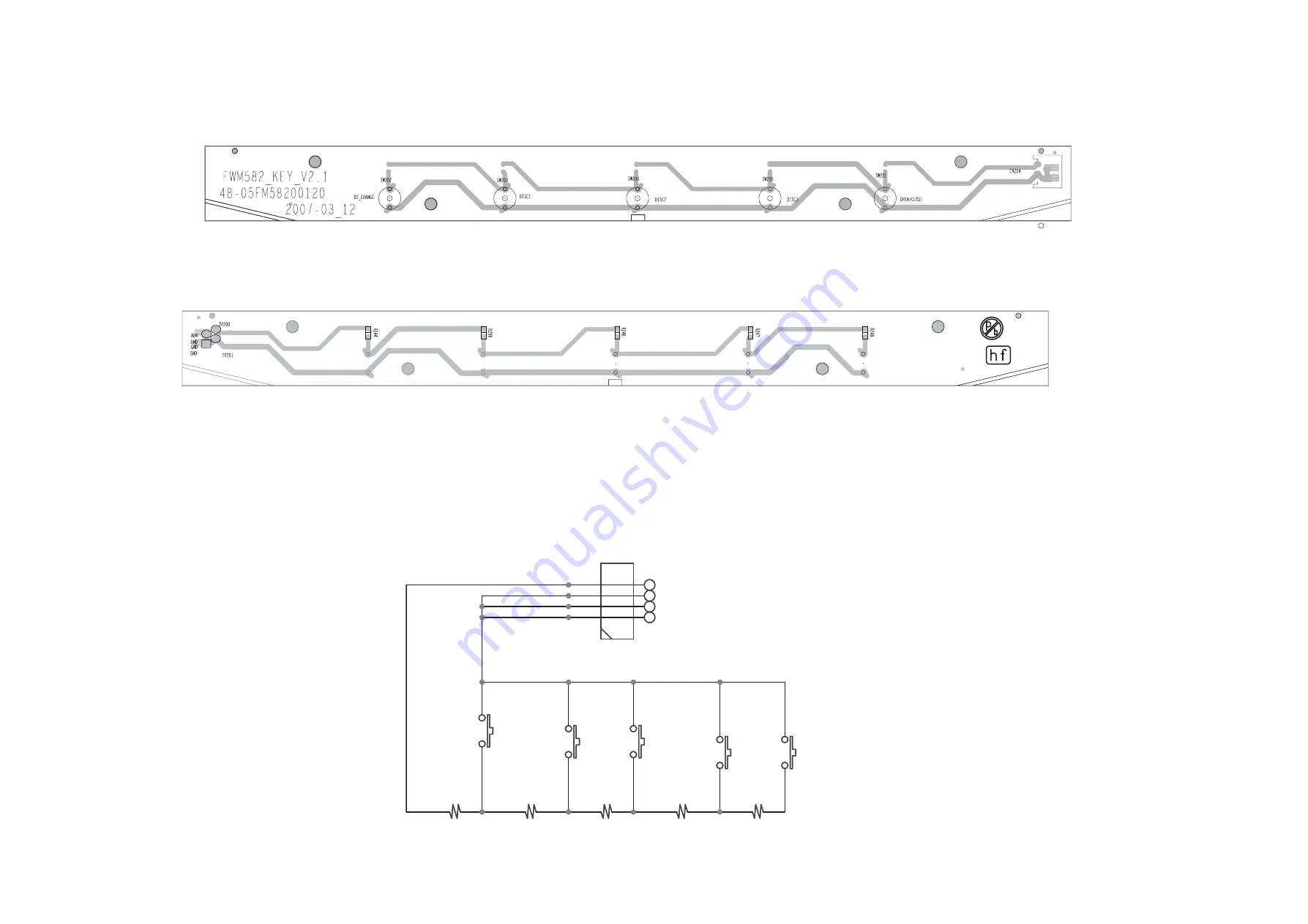
SW205
DISC3
SW205
DISC3
SW203
DISC1
SW203
DISC1
R249
120K
R249
120K
SW201
OPEN/CLOSE
SW201
OPEN/CLOSE
SW204
DISC2
SW204
DISC2
R244
5K6
R244
5K6
SW202
DS_CHANGE
SW202
DS_CHANGE
TP203
TP203
TP202
TP202
TP200
TP200
CN204
CON_4PIN_FFC_1.27mm
CN204
CON_4PIN_FFC_1.27mm
P1
1
P2
2
P3
3
P4
4
TP201
TP201
CIRCUIT DIAGRAM - KEY BOARD
Содержание FWM583
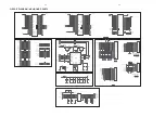
Страница 10: ...74HCT04D HEF4013BT 4 1 4 1 SET BLOCK DIAGRAM ...
Страница 11: ...4 2 4 2 SET WIRING DIAGRAM ...
Страница 12: ...5 1 5 1 PCB LAYOUT FRONT BOARD TOP VIEW ...
Страница 13: ...5 2 5 2 PCB LAYOUT FRONT BOARD BOTTOM VIEW ...
Страница 16: ...6 1 6 1 PCB LAYOUT MCU BOARD TOP VIEW ...
Страница 17: ...6 2 6 2 PCB LAYOUT MCU BOARD BOTTOM VIEW ...
Страница 20: ...9 1 9 1 LAYOUT DIAGRAM MAINS BOARD TOP VIEW ...
Страница 25: ...8 2 8 2 LAYOUT DIAGRAM CD BOARD TOP VIEW ...
Страница 26: ...8 3 8 3 LAYOUT DIAGRAM CD BOARD BOTTOM VIEW ...
Страница 29: ...9 1 9 1 LAYOUT DIAGRAM MAINS BOARD TOP VIEW ...
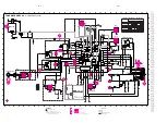
Страница 30: ...9 2 9 2 CIRCUIT DIAGRAM MAINS BOARD ...
Страница 31: ...9 3 9 3 LAYOUT DIAGRAM MIC BOARD TOP VIEW LAYOUT DIAGRAM MIC BOARD BOTTOM VIEW ...
Страница 33: ...10 1 10 1 LAYOUT DIAGRAM HIGH AMP USB JACK BOARD TOP VIEW ...
Страница 34: ...10 2 10 2 LAYOUT DIAGRAM HIGH AMP USB JACK BOARD BOTTOM VIEW ...
Страница 35: ...10 3 10 3 LAYOUT DIAGRAM POWER BOARD TOP VIEW ...
Страница 36: ...10 4 10 4 LAYOUT DIAGRAM POWER BOARD BOTTOM VIEW ...
Страница 37: ...CIRCUIT DIAGRAM HIGH AMP BOARD POWER BOARD 10 3 10 3 ...
Страница 41: ...12 4 12 4 SOURCE SELECTION SOUND PROCESSING CIRCUIT ...
Страница 42: ...12 5 12 5 HEADPHONE AMPLIFIER I2 C EXPANDER CIRCUIT 1K ...
Страница 44: ...SET MECHANICAL EXPLODED VIEW 13 1 13 1 ...