


Circuit-, IC descriptions and list of abbreviations
9.
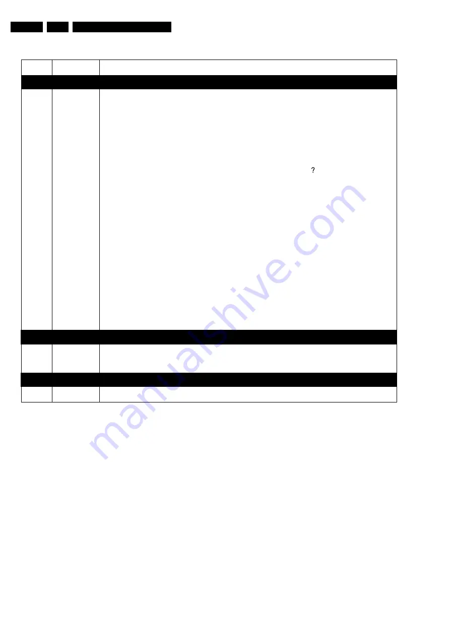
Pin #
Name
Description
SDRAM Interface Signals
125-131
ADDR
10-0
SDRAM Address bus. This signal bus is used to address the external SDRAM(s) used for
133-136
field memories. It should be connected to the A
10-0
bus of the memory chip(s). Please refer
to the Applications section of this data sheet for further details.
176-169
DATA
29-0
SDRAM Data bus. This signal bus is used to transfer the data to and from the external
166-160
SDRAM(s) used for field memories. It should be connected to the DQ
29-0
bus of the memory
157-153
chip when using a 64 Mbit SDRAM. When using two 16 Mbit SDRAMs this 30-bit bus may
150-146
be connected to the two 16-bit data busses of the memories in two ways: either connect 16
143-139
lines to one chip and 14 to the other, or connect 15 to both. In all cases the two unused data
lines on the memory chip(s) should be connected to ground via 22 k resistors. Please refer
to the Applications section of this data sheet for further details.
118
MEMCLKO
SDRAM clock and 2x output sampling clock. This clock is derived from PIXCLK and will be at
double the frequency of YCLKO. This active signal should be connected to the CLK pin(s) on
the SDRAM(s). When the 10-bit output mode selected the output signals will also change at
this clock rate and this should then be used as the output clock..
119
WEN
SDRAM Write Enable. This active low signal should be connected to the WE pin(s) on the
SDRAM(s).
120
RASN
SDRAM Row Address Select. This active low signal should be connected to the RAS pin(s)
on the SDRAM(s).
121
CASN
SDRAM Column Address Select. This active low signal should be connected to the CAS
pin(s) on the SDRAM(s).
122
BSEL
SDRAM Bank Select. When using two 16 Mbit SDRAMs this signal should be connected to
the BA (also called BS or A
11
) pin on both SDRAMs. When using a 64 Mbit SDRAM this
signal should be connected to the BA0 (also called BS0 or A
11
) pin on the SDRAM and BA1/
BS1 (also called BA when BA0 is referred to as A
11
) should be tied low.
Test Inputs
41, 50,
TEST
4-0
These pins are used for test purposes only and should always be tied low for normal operation.
51, 109,
111
Test Outputs
112, 113 TESTO
1-0
These pins are test outputs and should be left unconnected in normal operation.
Содержание DVDR70/001
Страница 88: ...Diagnostic Software EN 88 DVDR70 DVDR75 0x1 5 ...
Страница 99: ...Block Diagrams Waveforms Wiring Diagram EN 99 DVDR70 DVDR75 0x1 6 Test points overview DIVIO Board ...
Страница 120: ...EN 120 DVDR70 DVDR75 0x1 7 Circuit Diagrams and PWB Layouts Layout Analog Board 603 3033 Top View TR 07014_001 120303 ...
Страница 124: ...EN 124 DVDR70 DVDR75 0x1 7 Circuit Diagrams and PWB Layouts Layout Analog Board 603 3028 Top View TR 07016_001 120303 ...
Страница 130: ...EN 130 DVDR70 DVDR75 0x1 7 Circuit Diagrams and PWB Layouts Layout UP Sub Board Top View TR 06012_001 040203 ...
Страница 137: ...Circuit Diagrams and PWB Layouts EN 137 DVDR70 DVDR75 0x1 7 Layout DVIO Board Overview Top View ...
Страница 138: ...EN 138 DVDR70 DVDR75 0x1 7 Circuit Diagrams and PWB Layouts Layout DVIO Board Part 1 Top View ...
Страница 139: ...Circuit Diagrams and PWB Layouts EN 139 DVDR70 DVDR75 0x1 7 Layout DVIO Board Part 2 Top View ...
Страница 166: ...EN 166 DVDR70 DVDR75 0x1 7 Circuit Diagrams and PWB Layouts ...
Страница 194: ...Circuit IC descriptions and list of abbreviations EN 194 DVDR70 DVDR75 0x1 9 Figure 9 15 ...
Страница 195: ...Circuit IC descriptions and list of abbreviations EN 195 DVDR70 DVDR75 0x1 9 Figure 9 16 ...
Страница 199: ...Circuit IC descriptions and list of abbreviations EN 199 DVDR70 DVDR75 0x1 9 IC7411 NJM2285 Analog Board Video Switch ...
Страница 220: ...Circuit IC descriptions and list of abbreviations EN 220 DVDR70 DVDR75 0x1 9 ...
Страница 221: ...Circuit IC descriptions and list of abbreviations EN 221 DVDR70 DVDR75 0x1 9 ...
Страница 223: ...Circuit IC descriptions and list of abbreviations EN 223 DVDR70 DVDR75 0x1 9 ...
Страница 224: ...Circuit IC descriptions and list of abbreviations EN 224 DVDR70 DVDR75 0x1 9 ...
Страница 225: ...Circuit IC descriptions and list of abbreviations EN 225 DVDR70 DVDR75 0x1 9 ...
Страница 226: ...Circuit IC descriptions and list of abbreviations EN 226 DVDR70 DVDR75 0x1 9 ...
Страница 227: ...Circuit IC descriptions and list of abbreviations EN 227 DVDR70 DVDR75 0x1 9 ...
Страница 228: ...Circuit IC descriptions and list of abbreviations EN 228 DVDR70 DVDR75 0x1 9 ...
Страница 229: ...Circuit IC descriptions and list of abbreviations EN 229 DVDR70 DVDR75 0x1 9 ...
Страница 231: ...Circuit IC descriptions and list of abbreviations EN 231 DVDR70 DVDR75 0x1 9 ...
Страница 232: ...Circuit IC descriptions and list of abbreviations EN 232 DVDR70 DVDR75 0x1 9 ...
Страница 233: ...Circuit IC descriptions and list of abbreviations EN 233 DVDR70 DVDR75 0x1 9 ...
Страница 234: ...Circuit IC descriptions and list of abbreviations EN 234 DVDR70 DVDR75 0x1 9 IC7605 BU2288FV DVIO Board Clock Divider ...
Страница 235: ...Circuit IC descriptions and list of abbreviations EN 235 DVDR70 DVDR75 0x1 9 ...
Страница 236: ...Circuit IC descriptions and list of abbreviations EN 236 DVDR70 DVDR75 0x1 9 IC7604 BA7082F DVIO Board PLL IC ...
Страница 237: ...Circuit IC descriptions and list of abbreviations EN 237 DVDR70 DVDR75 0x1 9 ...
Страница 238: ...Circuit IC descriptions and list of abbreviations EN 238 DVDR70 DVDR75 0x1 9 ...


