


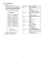


2 Warning
2.1.
Prevention of Electrostatic Discharge (ESD) to Electrostatically
Sensitive (ES) Devices
Some semiconductor (solid state) devices can be damaged easily by static electricity. Such components commonly are called Elec
trostatically Sensitive (ES) Devices. Examples of typical ES devices are integrated circuits and some field-effect transistors and
semiconductor [chip] components. The following techniques should be used to help reduce the incidence of component damage
caused by electrostatic discharge (ESD).
1. Immediately before handling any semiconductor component or semiconductor-equipped assembly, drain off any ESD on your
body by touching a known earth ground. Alternatively, obtain and wear a commercially available discharging ESD wrist strap,
which should be removed for potential shock reasons prior to applying power to the unit under test.
2. After removing an electrical assembly equipped with ES devices, place the assembly on a conductive surface such as alumi
num foil, to prevent electrostatic charge buildup or exposure of the assembly.
3. Use only a grounded-tip soldering iron to solder or unsolder ES devices.
4. Use only an anti-static solder removal device. Some solder removal devices not classified as [anti-static (ESD protected)] can
generate electrical charge sufficient to damage ES devices.
5. Do not use freon-propelled chemicals. These can generate electrical charges sufficient to damage ES devices.
6. Do not remove a replacement ES device from its protective package until immediately before you are ready to install it. (Most
replacement ES devices are packaged with leads electrically shorted together by conductive foam, aluminum foil or compara
ble conductive material).
7. Immediately before removing the protective material from the leads of a replacement ES device, touch the protective material
to the chassis or circuit assembly into which the device will be installed.
Caution
Be sure no power is applied to the chassis or circuit, and observe all other safety precautions.
8. Minimize bodily motions when handling unpackaged replacement ES devices. (Otherwise ham less motion such as the brush
ing together of your clothes fabric or the lifting of your foot from a carpeted floor can generate static electricity (ESD) sufficient
to damage an ES device).
4
Содержание Viera TC-P50C2
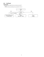
Страница 19: ...6 4 No Picture Input only y v h a t s lnPut 0Г 1 У Signal 19 ...
Страница 32: ...32 ...
Страница 33: ...10 Block Diagram 10 1 Main Block Diagram A D IG ITAL SIG NAL PROCESSO R 33 ...
Страница 34: ...10 2 Block 1 4 Diagram ...
Страница 35: ...10 3 Block 2 4 Diagram A D IG ITAL SIG N AL PROCESSO R 35 ...
Страница 36: ...10 4 Block 3 4 Diagram I p PO W ER SUPPLY 36 ...
Страница 37: ...10 5 Block 4 4 Diagram s C s c a n d r iv e SS SU STAIN DRIVE PLASMA PANEL PANEL SUSIAIN ELECTRODE 37 ...
Страница 38: ...38 ...
Страница 40: ...11 3 Wiring 2 40 ...
Страница 41: ...11 4 Wiring 3 41 ...
Страница 42: ...42 ...
Страница 47: ...14 15 16 17 18 45 ...
Страница 49: ...24 25 26 27 ...
Страница 50: ...12 5 А Board 4 14 Schematic Diagram A A B O A R D TXN A1 LNUUS 4 14 P O W E R SU P P LY 28 29 30 31 32 47 ...
Страница 52: ...12 6 А Board 5 14 Schematic Diagram A A B O A R D TXN A1 LNUUS 5 14 A V S W PC M O D EL TO 1 14 r 37 38 39 40 ...
Страница 56: ...12 9 A Board 8 14 Schematic Diagram A A B O A R D TXN A 1LN U U S 8 14 HDMI 64 65 66 67 68 69 70 71 72 51 ...
Страница 57: ...12 10 A Board 9 14 Schematic Diagram 52 ...
Страница 59: ...12 12 A Board 11 14 Schematic Diagram A 91 92 93 94 95 96 97 98 99 TO 1 6 10 14 54 0 0 0 ...
Страница 60: ...12 13 A Board 12 14 Schematic Diagram 100 1 101 1 102 1 103 1 104 1 105 1 106 1 107 1 108 55 ...
Страница 62: ...12 15 A Board 14 14 Schematic Diagram Ш 222 TO A34 C2 BOARD C21 118 119 120 121 122 123 124 126 126 57 ...
Страница 63: ...12 16 C1 Board Schematic Diagram D A C1 B O A R D T X N C 11LNUU 58 ...
Страница 64: ...1 I Н X I I H I I I 6 7 8 9 ...
Страница 65: ...12 17 C2 Board Schematic Diagram A C D B E F i 2 3 4 8 9 5 59 ...
Страница 66: ...12 18 SC Board 1 4 Schematic Diagram A C D A S C BO AR D TX N S C 1LN U U 1 4 TO B E F 1 2 3 4 6 8 9 5 7 60 ...
Страница 67: ...12 19 SC Board 2 4 Schematic Diagram 10 11 12 13 14 15 16 17 18 61 ...
Страница 68: ...12 20 SC Board 3 4 Schematic Diagram A S C BO AR D TXN S C 1LN U U 3 4 19 20 21 22 23 24 25 26 27 62 ...
Страница 69: ...12 21 SC Board 4 4 Schematic Diagram A S C BO AR D TXN S C 1LN U U 4 4 28 29 30 31 32 33 34 35 36 63 ...
Страница 70: ...12 22 SS Board 1 2 Schematic Diagram A C D A B E F 6 5 7 64 ...
Страница 73: ...S BOARD FOIL SIDE TXN S1EQUUM S BOARD COMPONENT SIDE TXN S1EQUUM F I G I H ...
Страница 74: ...Z9 9 SnnNI l V NXl aais nod aavoa v pjeog v Z ZV ...
Страница 75: ...68 ...
Страница 77: ...13 4 C2 Board 6 3 C2 BOARD COMPONENT SIDE TXNC21LNUU 70 ...
Страница 78: ...13 5 SC Board 71 ...
Страница 79: ...SC BOARD COMPONENT SIDE TXNSC1LNUU G 6 5 4 3 2 1 E F H 72 ...
Страница 80: ...13 6 SS Board 6 5 4 SS BOARD FOIL SIDE TXNSS1LNUU ...
Страница 81: ...1 I F I G I H 73 ...
Страница 82: ...6 5 4 SS BOARD COMPONENT SIDE TXNSS1LNUU A В С D ...
Страница 83: ...74 ...
Страница 85: ...14 1 2 Exploded View 2 76 ...
Страница 86: ...14 1 3 Accessories 77 ...


