
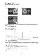


1. Remove the SU-Board and SD-Board. (See section 8.
and 8.9.)
2. Unlock the cable clampers to free the cable.
3. Disconnect the connectors (SC2 and SC3).
4. Disconnect the flexible cable (SC20).
5. Remove the screws (x8
and remove the SC-Board.
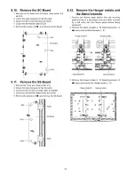
8.10. Remove the SC-Board
8.11. Remove the SS-Board
1. Remove the Tuner unit. (See section 8.5.)
2. Unlock the cable clampers to free the cable.
3. Disconnect the connectors (SS3, SS11 and SS23).
4. Disconnect the flexible cables (SS52 and SS55).
5. Remove the screws (x4
and remove the SS-Board.
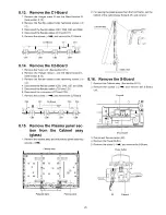
8.12. Remove the Hanger metals and
the Stand brackets
1. Remove the Plasma panel section from the servicing
stand and lay on a flat surface such as a table (covered
by a soft cloth) with the Plasma panel surface facing
downward.
2. Remove the Stand brackets (L, R) fastening screws (x3
^ each) and the Stand brackets (L, R).
3. Remove the Hanger metals (L, R) fastening screws (x2
^ each) and remove the Hanger metals (L, R).
24
Содержание Viera TC-P50C2
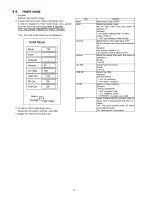
Страница 19: ...6 4 No Picture Input only y v h a t s lnPut 0Г 1 У Signal 19 ...
Страница 32: ...32 ...
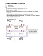
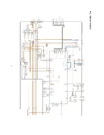
Страница 33: ...10 Block Diagram 10 1 Main Block Diagram A D IG ITAL SIG NAL PROCESSO R 33 ...
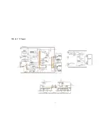
Страница 34: ...10 2 Block 1 4 Diagram ...
Страница 35: ...10 3 Block 2 4 Diagram A D IG ITAL SIG N AL PROCESSO R 35 ...
Страница 36: ...10 4 Block 3 4 Diagram I p PO W ER SUPPLY 36 ...
Страница 37: ...10 5 Block 4 4 Diagram s C s c a n d r iv e SS SU STAIN DRIVE PLASMA PANEL PANEL SUSIAIN ELECTRODE 37 ...
Страница 38: ...38 ...
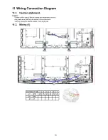
Страница 40: ...11 3 Wiring 2 40 ...
Страница 41: ...11 4 Wiring 3 41 ...
Страница 42: ...42 ...
Страница 47: ...14 15 16 17 18 45 ...
Страница 49: ...24 25 26 27 ...
Страница 50: ...12 5 А Board 4 14 Schematic Diagram A A B O A R D TXN A1 LNUUS 4 14 P O W E R SU P P LY 28 29 30 31 32 47 ...
Страница 52: ...12 6 А Board 5 14 Schematic Diagram A A B O A R D TXN A1 LNUUS 5 14 A V S W PC M O D EL TO 1 14 r 37 38 39 40 ...
Страница 56: ...12 9 A Board 8 14 Schematic Diagram A A B O A R D TXN A 1LN U U S 8 14 HDMI 64 65 66 67 68 69 70 71 72 51 ...
Страница 57: ...12 10 A Board 9 14 Schematic Diagram 52 ...
Страница 59: ...12 12 A Board 11 14 Schematic Diagram A 91 92 93 94 95 96 97 98 99 TO 1 6 10 14 54 0 0 0 ...
Страница 60: ...12 13 A Board 12 14 Schematic Diagram 100 1 101 1 102 1 103 1 104 1 105 1 106 1 107 1 108 55 ...
Страница 62: ...12 15 A Board 14 14 Schematic Diagram Ш 222 TO A34 C2 BOARD C21 118 119 120 121 122 123 124 126 126 57 ...
Страница 63: ...12 16 C1 Board Schematic Diagram D A C1 B O A R D T X N C 11LNUU 58 ...
Страница 64: ...1 I Н X I I H I I I 6 7 8 9 ...
Страница 65: ...12 17 C2 Board Schematic Diagram A C D B E F i 2 3 4 8 9 5 59 ...
Страница 66: ...12 18 SC Board 1 4 Schematic Diagram A C D A S C BO AR D TX N S C 1LN U U 1 4 TO B E F 1 2 3 4 6 8 9 5 7 60 ...
Страница 67: ...12 19 SC Board 2 4 Schematic Diagram 10 11 12 13 14 15 16 17 18 61 ...
Страница 68: ...12 20 SC Board 3 4 Schematic Diagram A S C BO AR D TXN S C 1LN U U 3 4 19 20 21 22 23 24 25 26 27 62 ...
Страница 69: ...12 21 SC Board 4 4 Schematic Diagram A S C BO AR D TXN S C 1LN U U 4 4 28 29 30 31 32 33 34 35 36 63 ...
Страница 70: ...12 22 SS Board 1 2 Schematic Diagram A C D A B E F 6 5 7 64 ...
Страница 73: ...S BOARD FOIL SIDE TXN S1EQUUM S BOARD COMPONENT SIDE TXN S1EQUUM F I G I H ...
Страница 74: ...Z9 9 SnnNI l V NXl aais nod aavoa v pjeog v Z ZV ...
Страница 75: ...68 ...
Страница 77: ...13 4 C2 Board 6 3 C2 BOARD COMPONENT SIDE TXNC21LNUU 70 ...
Страница 78: ...13 5 SC Board 71 ...
Страница 79: ...SC BOARD COMPONENT SIDE TXNSC1LNUU G 6 5 4 3 2 1 E F H 72 ...
Страница 80: ...13 6 SS Board 6 5 4 SS BOARD FOIL SIDE TXNSS1LNUU ...
Страница 81: ...1 I F I G I H 73 ...
Страница 82: ...6 5 4 SS BOARD COMPONENT SIDE TXNSS1LNUU A В С D ...
Страница 83: ...74 ...
Страница 85: ...14 1 2 Exploded View 2 76 ...
Страница 86: ...14 1 3 Accessories 77 ...


