Note: Lead is listed as (Pb) in the periodic table o f elements.
In the information below, Pb will refer to Lead solder, and PbF will refer to Lead Free Solder.
The Lead Free Solder used in our manufacturing process and discussed below is (Sn+Ag+Cu).
That is Tin (Sn), Silver (Ag) and Copper (Cu) although other types are available.
This model uses Pb Free solder in it's manufacture due to environmental conservation issues. For service and repair work, we'd
suggest the use of Pb free solder as well, although Pb solder may be used.
PCBs manufactured using lead free solder will have the PbF within a leaf Symbol
PbF
stamped on the back of PCB.
Caution
• Pb free solder has a higher melting point than standard solder. Typically the melting point is 50 ~ 70 °F (30~40 °C) higher. Please
use a high tem perature soldering iron and set it to 700 ± 20 °F (370 ± 10 °C).
• Pb free solder will tend to splash when heated too high (about 1100 °F or 600 °C).
If you must use Pb solder, please completely remove all of the Pb free solder on the pins or solder area before applying Pb sol
der. If this is not practical, be sure to heat the Pb free solder until it melts, before applying Pb solder.
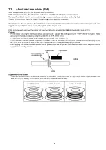
• A fter applying PbF solder to double layered boards, please check the com ponent side for excess solder which may flow onto the
opposite side. (see figure below)
component
component
remove all of the
^ 1П\
excess solder
2.2.
About lead free solder (PbF)
slice
\
solder
Suggested Pb free solder
There are several kinds of Pb free solder available for purchase. This product uses Sn+Ag+Cu (tin, silver, copper) solder. How
ever, Sn+Cu (tin, copper), Sn+Zn+Bi (tin, zinc, bismuth) solder can also be used.
5
Содержание TX-PR37C10
Страница 16: ...6 4 No Picture No Picture Check NG 16 ...
Страница 26: ...8 1 4 Adjustment Volume Location 8 1 5 VR16600 Vad Test Point Location 26 ...
Страница 31: ...9 Block Diagram 9 1 Main Block Diagram 31 ...
Страница 32: ...9 2 Block 1 3 Diagram JK8302 SPEAKER L SPEAKER R SD CARD SLOT 32 ...
Страница 33: ...9 3 Block 2 3 Diagram RM2501 REMOTE 33 ...
Страница 34: ...9 4 Block 3 3 Diagram s s s u s t a i n d r iv e P O W E R S U P P LY s c s c a n d r i v e 34 ...
Страница 36: ...10 3 Wiring 2 36 ...
Страница 38: ...38 ...
Страница 41: ...11 2 P Board 1 4 Schematic Diagram 40 0 ...
Страница 42: ... 0 11 3 P Board 2 4 Schematic Diagram TO A BOARD A25 T O P B O A R D 4 4 10 11 12 13 14 15 16 17 18 41 ...
Страница 43: ...11 4 P Board 3 4 Schematic Diagram A B C D E A P BOARD LSEP1279BEHB 3 4 F 1 2 3 4 42 ...
Страница 44: ... 11 5 P Board 4 4 Schematic Diagram 10 1 11 1 12 1 13 1 14 1 15 1 16 1 17 1 18 43 ...
Страница 45: ...11 6 GK К and S Board Schematic Diagram A С F 1 2 3 ...
Страница 46: ...S BOARD TXN S1 ETUE ...
Страница 47: ...11 7 A Board 1 21 Schematic Diagram A A A BOARD 1 21 IIC REF No 0900 0999 F 3 4 5 45 ...
Страница 50: ...11 10 A Board 4 21 Schematic Diagram A A BOARD 4 21 ADV_V REF No 4500 4799 28 29 30 31 32 33 34 35 36 48 ...
Страница 51: ...11 11 A Board 5 21 Schematic Diagram 37 38 39 40 ...
Страница 52: ...А A BOARD 5 21 ADV_V REF No 4500 4799 41 42 43 44 45 49 ...
Страница 53: ...11 12 A Board 6 21 Schematic Diagram TO 6 71 46 47 48 49 50 50 ...
Страница 54: ...А A BOARD 6 21 ADV_A REF No 2000 2499 51 52 53 54 ...
Страница 55: ...11 13 A Board 7 21 Schematic Diagram 55 56 57 58 59 60 61 62 63 51 ...
Страница 56: ...11 14 A Board 8 21 Schematic Diagram TO 7 21 A A BOARD 8 21 A V S W REF No 3000 3399 64 65 66 67 ...
Страница 57: ...ТО 9 21 ТО 7 21 68 69 70 71 72 52 ...
Страница 61: ...11 18 A Board 12 21 Schematic Diagram 100 101 102 103 104 105 106 107 108 56 ...
Страница 62: ... 0 11 19 A Board 13 21 Schematic Diagram 109 1 110 1 111 1 112 1 113 1 114 1 115 1 116 1 117 57 ...
Страница 63: ...11 20 A Board 14 21 Schematic Diagram DO W N LEFT 118 119 120 121 122 123 124 125 126 58 ...
Страница 68: ...11 25 A Board 19 21 Schematic Diagram A A BOARD 19 21 DTV CRNo 8300 8999 163 164 165 166 ...
Страница 69: ...63 ...
Страница 70: ...11 26 A Board 20 21 Schematic Diagram 172 A BOARD 20 21 DTV CRNo 8300 8999 173 174 175 176 177 178 179 180 64 ...
Страница 71: ...11 27 A Board 21 21 Schematic Diagram A A BOARD 21 21 DTV 181 182 183 184 185 186 187 188 189 65 ...
Страница 73: ...11 29 C1 Board 2 2 Schematic Diagram A C 10 C2 BOARD 18 10 11 12 13 14 15 16 17 C1 BOARD TN PA4890 2 2 67 ...
Страница 74: ...11 30 C2 Board 1 2 Schematic Diagram A C2 BOARD TNPA4891 1 2 TO A BOARD A31 C21 л B 68 ...
Страница 75: ...11 31 C2 Board 2 2 Schematic Diagram TO A BOARD A32 10 11 12 13 14 15 16 17 18 69 ...
Страница 76: ...11 32 SC Board 1 3 Schematic Diagram в D A SC BOARD TXNSC1 ERUE 1 3 1 2 3 4 ...
Страница 77: ...IC16771 C0CBADC00072 70 ...
Страница 78: ...11 33 SC Board 2 3 Schematic Diagram 10 11 12 13 14 15 16 17 18 71 ...
Страница 79: ...11 34 SC Board 3 3 Schematic Diagram 19 20 21 22 23 24 25 26 27 72 ...
Страница 80: ...11 35 SS Board 1 2 Schematic Diagram A B C D E F 3 4 5 73 ...
Страница 85: ...P BOARD COMPONENT SIDE LSEP1279BEHB 77 ...
Страница 87: ...K BOARD FOIL SIDE TXN K1ETUE K BOARD COMPONENT SIDE TXN K1 ETUE ...
Страница 88: ...12 3 A Board A BOARD FOIL SIDE A PR37C10 6 5 4 3 2 1 A I B I C I D I E I F I G I H I I 79 ...
Страница 91: ...A BOARD COMPONENT SIDE A PR37C10 81 ...
Страница 94: ...12 6 SC Board SC BOARD FOIL SIDE TXNSC1ERUE 6 5 4 3 2 1 A I B I C I D I E I F I G I H I I 84 ...
Страница 97: ...SC BOARD COMPONENT SIDE TXNSC1ERUE B G 6 5 4 3 2 1 E F H 86 ...
Страница 100: ......
Страница 102: ...13 1 2 Packing 1 90 ...
Страница 103: ...91 ...

