


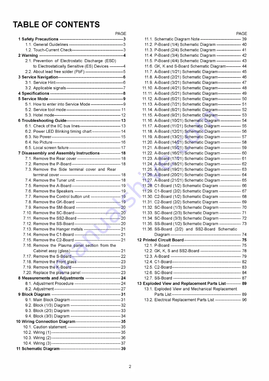
TABLE OF CONTENTS
1 Safety P re c a u tio n s -----------
1.1. General Guidelines —
1.2. Touch-Current C heck-
2 W a rn in g ----------------------------
PAGE
------
3
------
3
------
3
------
4
2.1. Prevention of Electrostatic Discharge (ESD)
to Electrostatically Sensitive (ES) D e v ic e s----------- 4
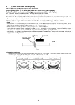
2.2. A bout lead free solder (P b F )------------------------------- 5
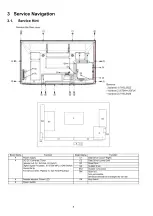
3 Service Navigation------------------------------------------------------ 6
3.1. Service H int-------------------------------------------------------- 6
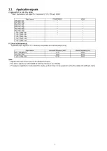
3.2. Applicable signals----------------------------------------------- 7
4 S pecifications------------------------------------------------------------- 8
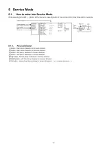
5 Service M o d e-------------------------------------------------------------- 9
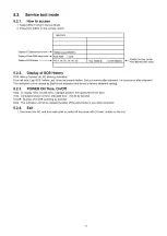
5.1. How to enter into Service M o d e --------------------------- 9
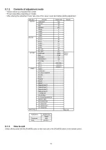
5.2. Service tool mode-
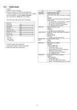
5.3. Hotel mode-----------
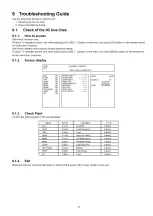
6 Troubleshooting Guide----------------------
6.1. Check of the IIC bus lines----------
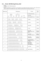
6.2. Power LED Blinking timing chart -
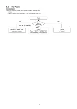
6.3. No P ower----------------------------------
6.4. No P icture--------------
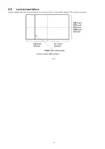
6.5. Local screen failure-
7 Disassem bly and A ssem bly Instructions
-
7.1. Remove the Rear c o v e r--------------------
7.2. Remove the P -B oard------------------------
11
12
13
13
14
15
16
17
18
18
18
7.3. Remove the Side terminal cover and Rear
terminal c o v e r----------------------------------------------------18
7.4. Remove the Tuner u n it-------------------------------------- 18
7.5. Remove the A -B o a rd ------------------------------------------19
7.6. Remove the S p e a ke rs--------------------------------------- 19
7.7. Remove the Control button u n it--------------------------19
7.8. Remove the G K -B o a rd -------------------------------------- 19
7.9. Remove the S M -B o a rd -------------------------------------- 20
7.10. Remove the SC-Board--------------------------------------- 20
7.11. Remove the S S 2-B oard------------------------------------- 20
7.12. Remove the S S-Board--------------------------------------- 20
7.13. Remove the Hanger m e ta ls --------------------------------21
7.14. Remove the C 1-B oard----------------------------------------21
7.15. Remove the C 2-B oard----------------------------------------21
7.16. Remove the Plasma panel section from the
Cabinet assy (glass)------------------------------------------- 21
7.17. Remove the S -B oard----------------------------------------- 22
7.18. Remove the Front g la s s -------------------------------------23
7.19. Remove the K -B oard----------------------------------------- 23
7.20. Replace the plasma panel --------------------------------- 23
------------------------------
8.1. Adjustm ent P rocedure--------------------------------------- 24
8.2. A djustm ent-------------------------------------------------------- 27
9 Block D ia g ra m -----------------------------------------------------------31
9.1. Main Block D iagram ------------------------------------------- 31
9.2. Block (1/3) Diagram -------------------------------------------32
9.3. Block (2/3) Diagram -------------------------------------------33
9.4. Block (3/3) Diagram -------------------------------------------34
10 Wiring Connection D iagram -------------------------------------- 35
10.1. Caution statem ent.---------------------------------------------35
10.2. W iring (1 )---------------------------------------------------------- 35
10.3. W iring (2 )---------------------------------------------------------- 36
10.4. W iring (3 )---------------------------------------------------------- 37
11 Schem atic Diagram ----------------------------------------------------39
11.1. Schematic Diagram Note-
11.2. P-Board
11.3. P-Board
11.4. P-Board
11.5. P-Board
11.6. GK, K and S-Board Schematic Diagram-
11.7. A-Board
11.8. A-Board
11.9. A-Board
11.10. A-Board
A-Board
.12. A-Board
.13. A-Board
.14. A-Board
.15. A-Board
.16. A-Board
.17. A-Board
.18. A-Board
.19. A-Board
.20. A-Board
A-Board
.22. A-Board
.23. A-Board
.24. A-Board
.25. A-Board
.26. A-Board
.27. A-Board
11.11
11
11
11
11
11
11
11
11
11
11
11
11
11
11
11
11
11
11
11
11
11
11
11
11
11
1/4) Schematic Diagram
2/4) Schematic Diagram
3/4) Schematic Diagram
4/4) Schematic Diagram
1/21)
2/21)
3/21)
4/21)
5/21)
6/21)
7/21)
8/21)
9/21)
10/21
11/21
12/21
13/21
14/21
15/21
16/21
17/21
18/21
19/21
20/21
21/21
Schematic Diagram----------------
Schematic Diagram----------------
Schematic Diagram----------------
Schematic Diagram----------------
Schematic Diagram----------------
Schematic Diagram----------------
Schematic Diagram----------------
Schematic Diagram----------------
Schematic Diagram----------------
) Schematic Diagram --------------
) Schematic Diagram --------------
) Schematic Diagram --------------
) Schematic Diagram --------------
) Schematic Diagram --------------
) Schematic Diagram --------------
) Schematic Diagram --------------
) Schematic Diagram --------------
) Schematic Diagram --------------
) Schematic Diagram --------------
) Schematic Diagram --------------
) Schematic Diagram --------------
28. C1-Board (1/2) Schematic D ia g ra m ----------------
29. C1-Board (2/2) Schematic Diagram ---------------
30. C2-Board (1/2) Schematic D ia g ra m ----------------
31. C2-Board (2/2) Schematic D ia g ra m ----------------
32. SC-Board (1/3) Schematic Diagram ---------------
33. SC-Board (2/3) Schematic Diagram ---------------
34. SC-Board (3/3) Schematic Diagram ---------------
35. SS-Board (1/2) Schematic D ia g ra m ----------------
36. SS-Board (2/2) and SS2-Board Schematic
Diagram --------------------------------------------------------
PAGE
---- 39
---- 40
---- 41
---- 42
---- 43
---- 44
---- 45
---- 46
---- 47
---- 48
---- 49
---- 50
---- 51
---- 52
---- 53
---- 54
---- 55
---- 56
---- 57
---- 58
---- 59
---- 60
---- 61
---- 62
---- 63
---- 64
---- 65
---- 66
---- 67
---- 68
---- 69
---- 70
---- 71
---- 72
---- 73
12 Printed Circuit Board
-
12.1. P -B o a rd ------------
12.2. GK, K, S and SS2-Board ■
12.3. A -B o a rd -------------------------
12.4. C1-Board------------------------
12.5. C2-Board------------------------
12.6. S C -B o a rd ----------------------
12.7. S S -B o a rd ----------------------
13 Exploded View and Replacem ent Parts List-
13.1. Exploded View and Mechanical Replacement
Parts L is t-------------------------------------------------------
13.2. Electrical Replacement Parts L is t-------------------
74
75
75
78
79
82
83
84
87
89
89
96
2
Содержание TX-PR37C10
Страница 16: ...6 4 No Picture No Picture Check NG 16 ...
Страница 26: ...8 1 4 Adjustment Volume Location 8 1 5 VR16600 Vad Test Point Location 26 ...
Страница 31: ...9 Block Diagram 9 1 Main Block Diagram 31 ...
Страница 32: ...9 2 Block 1 3 Diagram JK8302 SPEAKER L SPEAKER R SD CARD SLOT 32 ...
Страница 33: ...9 3 Block 2 3 Diagram RM2501 REMOTE 33 ...
Страница 34: ...9 4 Block 3 3 Diagram s s s u s t a i n d r iv e P O W E R S U P P LY s c s c a n d r i v e 34 ...
Страница 36: ...10 3 Wiring 2 36 ...
Страница 38: ...38 ...
Страница 41: ...11 2 P Board 1 4 Schematic Diagram 40 0 ...
Страница 42: ... 0 11 3 P Board 2 4 Schematic Diagram TO A BOARD A25 T O P B O A R D 4 4 10 11 12 13 14 15 16 17 18 41 ...
Страница 43: ...11 4 P Board 3 4 Schematic Diagram A B C D E A P BOARD LSEP1279BEHB 3 4 F 1 2 3 4 42 ...
Страница 44: ... 11 5 P Board 4 4 Schematic Diagram 10 1 11 1 12 1 13 1 14 1 15 1 16 1 17 1 18 43 ...
Страница 45: ...11 6 GK К and S Board Schematic Diagram A С F 1 2 3 ...
Страница 46: ...S BOARD TXN S1 ETUE ...
Страница 47: ...11 7 A Board 1 21 Schematic Diagram A A A BOARD 1 21 IIC REF No 0900 0999 F 3 4 5 45 ...
Страница 50: ...11 10 A Board 4 21 Schematic Diagram A A BOARD 4 21 ADV_V REF No 4500 4799 28 29 30 31 32 33 34 35 36 48 ...
Страница 51: ...11 11 A Board 5 21 Schematic Diagram 37 38 39 40 ...
Страница 52: ...А A BOARD 5 21 ADV_V REF No 4500 4799 41 42 43 44 45 49 ...
Страница 53: ...11 12 A Board 6 21 Schematic Diagram TO 6 71 46 47 48 49 50 50 ...
Страница 54: ...А A BOARD 6 21 ADV_A REF No 2000 2499 51 52 53 54 ...
Страница 55: ...11 13 A Board 7 21 Schematic Diagram 55 56 57 58 59 60 61 62 63 51 ...
Страница 56: ...11 14 A Board 8 21 Schematic Diagram TO 7 21 A A BOARD 8 21 A V S W REF No 3000 3399 64 65 66 67 ...
Страница 57: ...ТО 9 21 ТО 7 21 68 69 70 71 72 52 ...
Страница 61: ...11 18 A Board 12 21 Schematic Diagram 100 101 102 103 104 105 106 107 108 56 ...
Страница 62: ... 0 11 19 A Board 13 21 Schematic Diagram 109 1 110 1 111 1 112 1 113 1 114 1 115 1 116 1 117 57 ...
Страница 63: ...11 20 A Board 14 21 Schematic Diagram DO W N LEFT 118 119 120 121 122 123 124 125 126 58 ...
Страница 68: ...11 25 A Board 19 21 Schematic Diagram A A BOARD 19 21 DTV CRNo 8300 8999 163 164 165 166 ...
Страница 69: ...63 ...
Страница 70: ...11 26 A Board 20 21 Schematic Diagram 172 A BOARD 20 21 DTV CRNo 8300 8999 173 174 175 176 177 178 179 180 64 ...
Страница 71: ...11 27 A Board 21 21 Schematic Diagram A A BOARD 21 21 DTV 181 182 183 184 185 186 187 188 189 65 ...
Страница 73: ...11 29 C1 Board 2 2 Schematic Diagram A C 10 C2 BOARD 18 10 11 12 13 14 15 16 17 C1 BOARD TN PA4890 2 2 67 ...
Страница 74: ...11 30 C2 Board 1 2 Schematic Diagram A C2 BOARD TNPA4891 1 2 TO A BOARD A31 C21 л B 68 ...
Страница 75: ...11 31 C2 Board 2 2 Schematic Diagram TO A BOARD A32 10 11 12 13 14 15 16 17 18 69 ...
Страница 76: ...11 32 SC Board 1 3 Schematic Diagram в D A SC BOARD TXNSC1 ERUE 1 3 1 2 3 4 ...
Страница 77: ...IC16771 C0CBADC00072 70 ...
Страница 78: ...11 33 SC Board 2 3 Schematic Diagram 10 11 12 13 14 15 16 17 18 71 ...
Страница 79: ...11 34 SC Board 3 3 Schematic Diagram 19 20 21 22 23 24 25 26 27 72 ...
Страница 80: ...11 35 SS Board 1 2 Schematic Diagram A B C D E F 3 4 5 73 ...
Страница 85: ...P BOARD COMPONENT SIDE LSEP1279BEHB 77 ...
Страница 87: ...K BOARD FOIL SIDE TXN K1ETUE K BOARD COMPONENT SIDE TXN K1 ETUE ...
Страница 88: ...12 3 A Board A BOARD FOIL SIDE A PR37C10 6 5 4 3 2 1 A I B I C I D I E I F I G I H I I 79 ...
Страница 91: ...A BOARD COMPONENT SIDE A PR37C10 81 ...
Страница 94: ...12 6 SC Board SC BOARD FOIL SIDE TXNSC1ERUE 6 5 4 3 2 1 A I B I C I D I E I F I G I H I I 84 ...
Страница 97: ...SC BOARD COMPONENT SIDE TXNSC1ERUE B G 6 5 4 3 2 1 E F H 86 ...
Страница 100: ......
Страница 102: ...13 1 2 Packing 1 90 ...
Страница 103: ...91 ...


