


S-1
S1. About Indication of The Schematic Diagram ............................ S-1
S1.1. Important Safety Notice......................................................... S-1
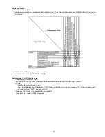
S2. Voltage Chart ........................................................................... S-2
S2.1. Rear P.C.B. ........................................................................... S-2
S2.2. Monitor P.C.B. ....................................................................... S-2
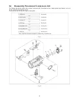
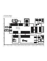
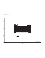
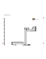
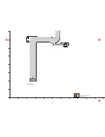
S3. Block Diagram .......................................................................... S-3
S3.1. Overall Block Diagram .......................................................... S-3
S4. Schematic Diagram .................................................................. S-4
S4.1. Interconnection Diagram ....................................................... S-4
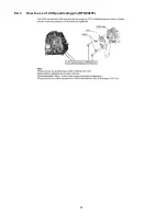
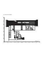
S4.2. Rear Schematic Diagram ...................................................... S-5
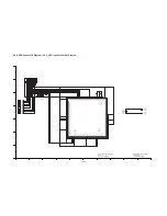
S4.3. CCD Schematic Diagram ...................................................... S-6
S4.4. EMC Schematic Diagram ...................................................... S-6
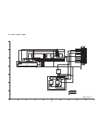
S4.5. DC BATT OP FPC Schematic Diagram ................................ S-7
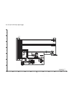
S4.6. MONI FPC Schematic Diagram ............................................ S-8
S4.7. Monitor Schematic Diagram .................................................. S-9
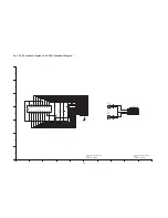
S4.8. ESD Schematic Diagram .................................................... S-10
S4.9. LED Light Schematic Diagram ............................................ S-10
S5. Print Circuit Board .................................................................. S-11
S5.1. Rear P.C.B. ......................................................................... S-11
S5.2. CCD P.C.B. ......................................................................... S-11
S5.3. EMC FPC P.C.B. ................................................................. S-12
S5.4. DC BATT OP FPC P.C.B. .................................................... S-12
S5.5. MONI FPC P.C.B. ................................................................ S-14
S5.6. Monitor P.C.B. ..................................................................... S-18
S5.7. ESD P.C.B. .......................................................................... S-19
S5.8. LED Light P.C.B. ................................................................. S-19
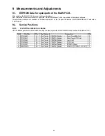
S6. Replacement Parts List .......................................................... S-21
S7. Exploded View ....................................................................... S-27
S7.1. Frame and Casing Section.................................................. S-27
S7.2. LCD Section ........................................................................ S-28
S7.3. Lens Section ....................................................................... S-29
S7.4. Packing Parts and Accessories Section .............................. S-30
Table of contents
Service Manual
VM100201
5
CE
Diagrams and Replacement
Parts List
Model No.
SD Video Camera
Vol. 1
Colour
(K)........Black Type (SDR-S50P/PC/EG/EF/EC/EP/EB/EE/GC/GA/GN/PU/PR,
T50P/PC/EG/EF/EC/EP/EB/EE/GC/GA, T51PU/PR, T55P/PC/EB/GC/GA, T56PU)
(A)........Blue Type (SDR-S50P/PC/EG/EF/EC/EB/EE/GN, T50PC, T55P)
(R)........Red Type (SDR-S50EG/EF/EC/EP/EB/EE/GC/GA/GN, T50PC/GC/GA, T51PU)
(P)........Pink Type (SDR-S50EG/EC/GC/GA, T50GC/GA/GK, T51PU, T55GK)
(W).......White Type (SDR-S50EG/EF/EC/EP/EB/GC/GA, T50GC/GA/GK, T55GK)
(H)........Gray Type (SDR-S50EB)
(N)........Gold Type (SDR-S50P/PC/EG/EP/EE/GC/GA, T50GC/GA/GK, T51PU/PR, T55P/GK)
SDR-T50P
SDR-T50PC
SDR-T50EG
SDR-T50EF
SDR-T50EC
SDR-T50EP
SDR-T50EB
SDR-T50EE
SDR-T50GC
SDR-T50GA
SDR-T50GK
SDR-T51PU
SDR-T51PR
SDR-T55P
SDR-T55PC
SDR-T55EB
SDR-T55GC
SDR-T55GA
SDR-T55GK
SDR-T56PU
SDR-S50P
SDR-S50PC
SDR-S50EG
SDR-S50EF
SDR-S50EC
SDR-S50EP
SDR-S50EB
SDR-S50EE
SDR-S50GC
SDR-S50GA
SDR-S50GN
SDR-S50PU
SDR-S50PR
Name of Signal
OFTR
FEP
This signal is connected
to the FEP schematic diagram.
Circuit name being connected.
6.Use the parts number indicated on the Replacement Parts List .
7.Indication on Schematic diagrams:
5.The voltage being indicated here may be include observational-error (deviation) due to
internal-resistance and/or reactance of equipment. Therefore, handle the value
indicated on here as reference.
4.Although the voltage and waveform available on here is measured with standard frame,
it may be differ from actual measurement due to modification of circuit and so on.
3.The voltage being indicated on the schematic diagram is measured in
"Standard-Playback" mode when there is no specify mode is mentioned.
2.It is only the "Test Round" and no terminal (Pin) is available on the P.C.B.
when the TP (Test Point) indicated as " " mark.
1.Although reference number of the parts is indicated on the P.C.B. drawing and/or
schematic diagrams, it is NOT mounted on the P.C.B. when it is displayed with "$" mark.
FOR SAFETY. WHEN REPLACING ANY OF THESE COMPONENTS USE ONLY THE SAME TYPE.
COMPONENTS IDENTIFIED WITH THE MARK
HAVE THE SPECIAL CHARACTERISTICS
S1. About Indication of The Schematic Diagram
S1.1. Important Safety Notice
Содержание SDR-S50P
Страница 11: ...11 4 Specifications...
Страница 13: ...13...
Страница 14: ...14...
Страница 18: ...18 7 Service Fixture Tools 7 1 Service Tools and Equipment...
Страница 21: ...21 Fig D3 Fig D4...
Страница 24: ...24 Fig D13 Fig D14 Fig D15 Fig D16...
Страница 25: ...25 Fig D17 Fig D18 Fig D19 Fig D20...
Страница 26: ...26 Fig D21 Fig D22...
Страница 28: ...28 8 4 1 How to use of CCD positioning pin RFKZ0476...
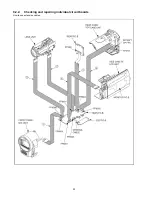
Страница 30: ...30 9 2 2 Checking and repairing individual circuit boards How to use extension cables...
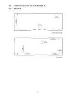
Страница 31: ...31 9 3 Location for Connectors of the Main P C B 9 3 1 Main P C B...
Страница 48: ...S 13...
Страница 49: ...S 14 S5 5 MONI FPC P C B FT901 1 2 S601 1 4 N M L K J I H G F E D SDR T55 T56 T51 T50 S50 MONI FPC P C B S 14...
Страница 50: ...S 15 2 4 SDR T55 T56 T51 T50 S50 MONI FPC P C B...
Страница 52: ...S 17 4 4 21 20 19 18 17 16 15 14 13 12 11 SDR T55 T56 T51 T50 S50 MONI FPC P C B...
Страница 55: ...S 20...
Страница 63: ...S7 2 LCD Section S 28 15 17 16 18 34 19 20 21 33 B17 B26 B27...