8.2.1. Operation
RF signal transmission and reception:
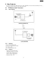
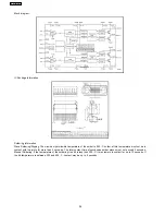
During the receive process, the radio signal is taken from a pair of balanced RF I/O pins that feed into the low noise amplifier (LNA).
Direct I/Q down conversion and on-chip filtering send the processed I/Q data to the analog-to-digital converter before processing
by the GFSK (Gaussian Frequency Shift Keying) demodulator. Within the demodulator, data detection and timing recovery circuits
convert the data for transfer to an external device. The transmit process operates in a similar fashion in reverse order.
The transmitted signal is GFSK (Gaussian Frequency Shift Keying) modulated data that is amplified on the chip to yield a radiated
output of 0dBm. A power control signal for an external amplifier is provided.
The audio baseband processor (C1BB00001102) is a digital audio processor IC encompassing apt-XTM audio
compress/decompress algorithm for wireless transmission of crystal-clear CD quality audio data.
For digital transmission the analog audio signals are sampled at 48kHz and converted to 1.536Mbps digital data through an
external 16-bit stereo audio codec. The digitized data are apt-XTM 4:1 compressed to 384Kbps stream data for efficient
transmission. Redundancy bits for forward error correction (FEC), synchronization flags, and control signals for time-division
duplexing (TDD) are appended to form data frames for error-free transmission.
In the receiver(Slave), synchronization flags and control data are first detected from the input stream. FEC decoder corrects any
errors that may have been introduced during the transmission and produces error-free compressed audio data. The compressed
audio is decompressed into 16-bit stereo PCM audio data through digital signal processing blocks. External audio codec converts
the PCM data to 2-channel (left and right) analog audio signals.
The Tx/Rx controller is in charge of several functions such as radio channel setup, frequency hopping for interference reduction and
generation of control signal for TDD and external RF chip.
In audio mode, the transmitter(Master) can send additional 16Kbps digital data simultaneously with stereo audio data.
How much time delay to transmit audio in wireless?
Audio compression and decompression requires about 3ms. Total time delay can be calculated as follows: Total delay time = audio
compression time + transmitter operating time + receiver operating time + audio decompression time. Total delay time is
approximately 12.2ms.
What is the power consumption?
The 2.4GHz RF module consumes about 45mA (max 65mA) for the transmitter and 55mA (max 71mA) for the receiver. The
EEPROM consumes about 1mA while the baseband IC consumes about 20mA. The total power consumption is 66mA (max 86mA)
for the transmitter and 76mA (max 92mA) for the receiver.
20
SA-HT640WPL
Содержание SA-HT640WPL
Страница 4: ...23 2 Packaging 109 24 Replacement Parts List 110 24 1 Component Parts List 111 4 SA HT640WPL ...
Страница 10: ...10 SA HT640WPL ...
Страница 16: ...16 SA HT640WPL ...
Страница 19: ...8 2 Detail Block Diagram Receiver module 19 SA HT640WPL ...
Страница 31: ...31 SA HT640WPL ...
Страница 37: ...10 1 Disassembly Flow Chart 37 SA HT640WPL ...
Страница 38: ...10 2 Main Components and P C B Locations 38 SA HT640WPL ...
Страница 46: ...Step 3 Push tray assembly to the direction of arrow shown 46 SA HT640WPL ...
Страница 53: ...14 2 Main P C B 53 SA HT640WPL ...
Страница 60: ...SA HT640WPL 60 ...
Страница 68: ...SA HT640WPL 68 ...
Страница 70: ...70 SA HT640WPL ...
Страница 80: ...SA HT640WPL 80 ...
Страница 86: ...SA HT640WPL 86 ...
Страница 88: ...SA HT640WPL 88 ...
Страница 97: ...97 SA HT640WPL ...
Страница 104: ...21 3 4 2 Receiver Module P C B 104 SA HT640WPL ...
Страница 106: ...23 Explode Views 23 1 Cabinet Parts Location 106 SA HT640WPL ...
Страница 107: ...107 SA HT640WPL ...
Страница 108: ...108 SA HT640WPL ...
Страница 109: ...23 2 Packaging 109 SA HT640WPL ...


