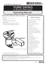


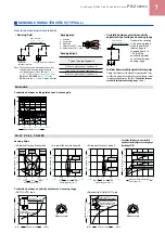


6
Long Range & Wide Area Photoelectric Sensor
PX-2
SERIES
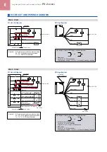
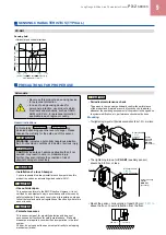
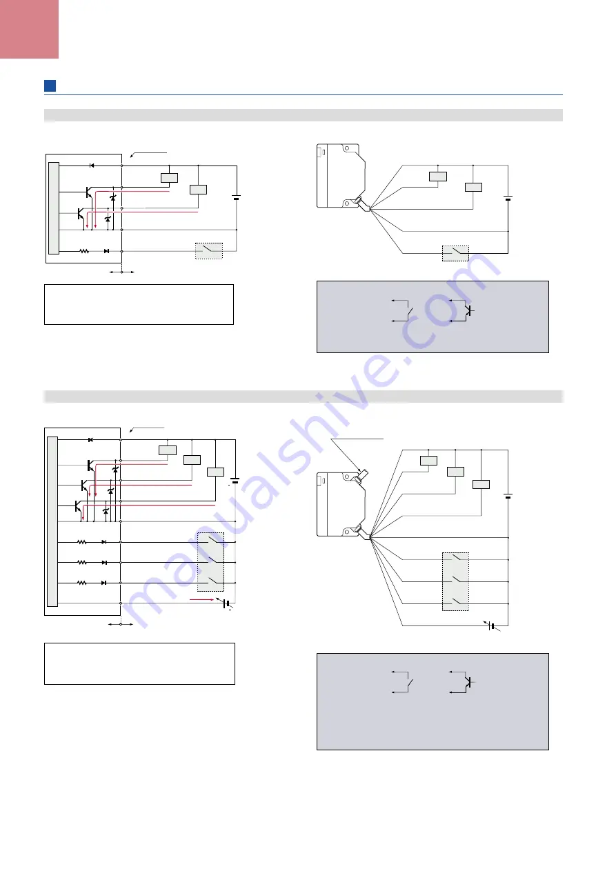
Sensor circuit
D
(Brown) +V
100 mA max.
Z
D1
Load
Z
D2
Load
(Black) OUT1
(White) OUT2
(Blue) 0 V
*1
Users’ circuit
Internal circuit
100 mA max.
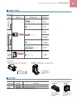
Color code
Tr
1
Tr
2
(Pink / Violet) Sleep input
+
-
10 to 31 V DC
Load
Brown
White
Black
Load
Blue
Pink / Violet
*1
+
-
10 to 31 V DC
I/O CIRCUIT AND WIRING DIAGRAMS
I/O circuit diagram
Wiring diagram
PX-22 PX-21
* 1
Non-voltage contact or NPN open-collector transistor
or
• Sleep input
Low (0 to 1 V): Sleep condition
High [(supply voltage – 1 V) to 31 V, or open]: Operating condition
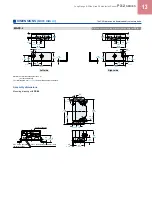
*1
Tr
1
Tr
2
Tr
3
D
100 mA max.
Z
D1
Z
D2
Z
D3
100 mA max.
100 mA max.
6 mA max.
Color code
Load
Load
Load
(Brown) +V
(White) OUT 2
(Black / White) Extraneous light monitor output
(Black) OUT 1
(Blue) 0 V
(Violet / Black) Auxiliary left
OUT 1 area ineffective input
(Pink / Violet) Sleep input
(Pink / Gray)
External sensitivity
adjustment input
Users’ circuit
Internal circuit
0 to +5 V DC
Sensor circuit
(Input impedance: 1 kΩ approx.)
(Violet) Auxiliary right
OUT 1 area ineffective input
10 to 31 V DC
+
+
For auxiliary
sensor connection
Load
Load
Load
Brown
Blue
White
Black / White
Black
Violet
Violet / Black
Pink / Gray
Pink / Violet
*1
0 to +5 V DC
+ -
+
-
10 to 31 V DC
PX-24 PX-26
I/O circuit diagram
Wiring diagram
* 1
Non-voltage contact or NPN open-collector transistor
or
• Auxiliary area ineffective input
Low (0 to 1 V): Area ineffective
High (4.5 to 31 V, or open): Area effective
• Sleep input
Low (0 to 1 V): Sleep condition
High [(supply voltage – 1 V) to 31 V, or open]: Operating condition
Symbols … D: Reverse supply polarity protection diode
Z
D1
, Z
D2
: Surge absorption zener diode
Tr
1
, Tr
2
: NPN output transistor
Symbols … D: Reverse supply polarity protection diode
Z
D1
, Z
D2
, Z
D3
: Surge absorption zener diode
Tr
1
, Tr
2
, Tr
3
: NPN output transistor