6.4.3. THERMAL HEAD
1. Function
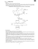
This unit utilizes the state of the art thermal printer technology.
The ink film is chemically processed. The ink film is comprised of two parts: an ink layer and a base film. When the thermalhead
contacts this ink film, it emits heat momentarily, and the ink layer is melted and transferred to the paper. If this continues, letters
and/or diagrams appear, and the original document is reproduced.
2. Circuit Operation
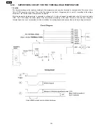
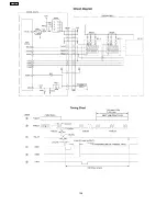
Refer to the block diagram and the timing chart on the following page.
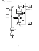
There are 27 driver ICs aligned horizontally on the thermal head and each one of these ICs can drive 64 heat-emitting registers.
This means that one line is at a density of 64×27=1728 dots=(8 dots/mm).
White/Black (white=0, black=1) data in one line increment is synchronized at IC501 pin 150 (THCLK), and sent from IC501 pin
149 (THDAT) to the shift register of the ICs. The shift registers of the 27 ICs are connected in series, and upon the shift of the
1728 dot increment, the shift register becomes filled with data, and a latch pulse is emitted to each IC from IC501 pin 151
(THLAT).
With this latch pulse, all the contents of the shift registers are latched to the latch registers. Thereafter, through the addition of
strobes from the IC501 pins (142, 143, 146), only the dot location of black (=1) among latched data activates the driver, and the
current passes to heat the emitting body to cause heat emission.
Here, the three line strobes, STB1 to STB3, impress at intervals of 9.216 msec, as required for one-line printout.
The sequence is shown on the next page. [Moreover, for the strobe width, the thermistor value inside the thermal head is
detected according to IC501 pin 2. Depending on that value, the strobe width is recorded in ROM (IC502). Accordingly, the
strobe width is determined.]
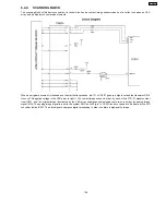
When the thermal head is not used, the IC501 (141, THON) becomes low , Q501 turns OFF, IC508 turns OFF, and the +24V
power supply for the thermal head driver is not impressed to protect the IC.
137
KX-FP101
Содержание KX-FP105BX
Страница 36: ...1 11 CCITT No 1 Test Chart Actual size 8 KX FP101 ...
Страница 38: ...1 12 2 CONTROL PANEL 10 KX FP101 ...
Страница 58: ...2 3 3 TROUBLESHOOTING ITEMS TABLE 30 KX FP101 ...
Страница 59: ...2 3 3 1 Simple Check List 31 KX FP101 ...
Страница 61: ...2 Document JAM 33 KX FP101 ...
Страница 63: ...4 Skew We recommend making a copy of the Fig B document in 3 Multiple feed and using it 35 KX FP101 ...
Страница 65: ...6 Paper JAM 7 Multiple feed and skew 37 KX FP101 ...
Страница 68: ...Fig C 12 A blank page is received 40 KX FP101 ...
Страница 72: ...2 3 3 3 1 Defective facsimile section 1 Transmit problem 44 KX FP101 ...
Страница 80: ...52 KX FP101 ...
Страница 81: ...53 KX FP101 ...
Страница 82: ...54 KX FP101 ...
Страница 83: ...55 KX FP101 ...
Страница 84: ...56 KX FP101 ...
Страница 85: ...57 KX FP101 ...
Страница 86: ...58 KX FP101 ...
Страница 87: ...59 KX FP101 ...
Страница 92: ...2 3 3 4 1 Digital Block Diagram 64 KX FP101 ...
Страница 95: ...I O and Pin No Diagram 67 KX FP101 ...
Страница 97: ...69 KX FP101 ...
Страница 98: ...NG Example 70 KX FP101 ...
Страница 99: ...2 3 3 4 2 Check the Status of the Digital Board 71 KX FP101 ...
Страница 101: ...Note Inside the digital board 73 KX FP101 ...
Страница 105: ...2 Troubleshooting Flow Chart 77 KX FP101 ...
Страница 107: ...2 3 3 7 Operation Panel Section 1 No key operation 2 No LCD indication 79 KX FP101 ...
Страница 109: ...5 Check the paper top sensor PS502 PAPER JAMMED 6 Check the film end sensor PS501 FILM EMPTY 81 KX FP101 ...
Страница 110: ...2 3 3 9 CIS Contact Image Sensor Section Refer to 6 4 4 SCANNING BLOCK 82 KX FP101 ...
Страница 111: ...83 KX FP101 ...
Страница 112: ...2 3 3 10 Thermal Head Section Refer to 6 4 3 THERMAL HEAD 84 KX FP101 ...
Страница 117: ...2 4 5 SERVICE MODE SETTINGS Example of a printed out list Note The above values are the default values 89 KX FP101 ...
Страница 125: ...2 4 7 3 PRINTOUT EXAMPLE 97 KX FP101 ...
Страница 126: ...98 KX FP101 ...
Страница 129: ...2 5 3 PRINT TEST PATTERN 1 Platen roller Reference pattern 101 KX FP101 ...
Страница 130: ...2 Left margin Top margin Reference pattern 102 KX FP101 ...
Страница 131: ...3 Thermal head 1 dot Reference pattern 103 KX FP101 ...
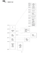
Страница 154: ...6 3 2 MEMORY MAP 126 KX FP101 ...
Страница 166: ...138 KX FP101 ...
Страница 176: ...6 4 6 3 2 Transmitting documents 6 4 6 3 3 Receiving FAX 148 KX FP101 ...
Страница 177: ...6 4 6 3 4 Copying 149 KX FP101 ...
Страница 188: ...b Redundancy Compression Process Coding Mode This unit uses one dimensional MH format 160 KX FP101 ...
Страница 212: ...12 1 MEMO KX FP101 184 ...
Страница 214: ...13 1 MEMO KX FP101 186 ...
Страница 216: ...14 1 MEMO KX FP101 188 ...
Страница 218: ...15 1 MEMO KX FP101 190 ...
Страница 220: ...16 1 MEMO KX FP101 192 ...
Страница 221: ...17 TERMINAL GUIDE OF THE IC S TRANSISTORS AND DIODES 193 KX FP101 ...
Страница 222: ...18 FIXTURES AND TOOLS 194 KX FP101 ...
Страница 223: ...19 CABINET MECHANICAL AND ELECTRICAL PARTS LOCATION 19 1 OPERATION PANEL SECTION 195 KX FP101 ...
Страница 224: ...19 2 UPPER CABINET SECTION 196 KX FP101 ...
Страница 225: ...19 2 1 PICK UP BASE SECTION 197 KX FP101 ...
Страница 226: ...19 3 LOWER P C B SECTION 198 KX FP101 ...
Страница 227: ...19 4 MOTOR SECTION 199 KX FP101 ...
Страница 228: ...19 5 ACTUAL SIZE OF SCREWS AND WASHER 200 KX FP101 ...
Страница 229: ...20 ACCESSORIES AND PACKING MATERIALS 201 KX FP101 ...
Страница 238: ...210 KX FP101 D Q KXFP101 Printed in Japan ...


