6.3.8.
SRAM AND RTC BACKUP CIRCUIT
1. Function
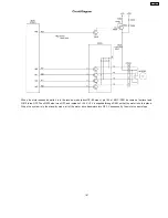
This unit has a lithium battery (BATT) which works for the SRAM (IC504) and Real Time Clock IC (RTC: inside IC501).
The user parameters for autodial numbers, the system setup data and others are stored in the SRAM (IC504).
The RTC continues to work, backed up by a lithium battery even when the power switch is OFF.
2. SRAM (IC504) Backup Circuit Operation
When the power switch is turned ON, power is supplied through pin 12 of IC501 to the SRAM (IC504). At this time, the voltage
at pin 28 of the SRAM is 5V. When the power switch is turned OFF, the BATT supplies power to the SRAM through J501, R562
and D504. The voltage at pin 28 of the SRAM is about +2.5V. When the power switch is OFF and the voltage of +5V decreases,
the voltage detect IC (IC509) outputs "Low " level and the IC501 outputs the reset signal. Pin 28 of the SRAM becomes roughly
the same voltage as the battery voltage. At this point, pin 20 (CS) of IC504 becomes high level, causing the SRAM to go into
the backup mode, in which the power consumption is lower.
3. RTC Inside (IC501) Backup Circuit Operation
When the power switch is turned ON, power is supplied through DA501 to the RTC (inside IC501). At this time, the voltage at
pin 7 of the IC501 is +3.3V. When the power switch is turned OFF, the BATT supplies power to RTC through DA501.
Thevoltage at pin 7 of IC501 is about +2.5V. When the power switch is OFF and the voltage of +3.3V decreases, pin 7 of RTC
(IC501) becomes roughly the same voltage as the battery voltage. RTC goes into the backup mode, in which the power
consumption is lower.
133
KX-FP101
Содержание KX-FP105BX
Страница 36: ...1 11 CCITT No 1 Test Chart Actual size 8 KX FP101 ...
Страница 38: ...1 12 2 CONTROL PANEL 10 KX FP101 ...
Страница 58: ...2 3 3 TROUBLESHOOTING ITEMS TABLE 30 KX FP101 ...
Страница 59: ...2 3 3 1 Simple Check List 31 KX FP101 ...
Страница 61: ...2 Document JAM 33 KX FP101 ...
Страница 63: ...4 Skew We recommend making a copy of the Fig B document in 3 Multiple feed and using it 35 KX FP101 ...
Страница 65: ...6 Paper JAM 7 Multiple feed and skew 37 KX FP101 ...
Страница 68: ...Fig C 12 A blank page is received 40 KX FP101 ...
Страница 72: ...2 3 3 3 1 Defective facsimile section 1 Transmit problem 44 KX FP101 ...
Страница 80: ...52 KX FP101 ...
Страница 81: ...53 KX FP101 ...
Страница 82: ...54 KX FP101 ...
Страница 83: ...55 KX FP101 ...
Страница 84: ...56 KX FP101 ...
Страница 85: ...57 KX FP101 ...
Страница 86: ...58 KX FP101 ...
Страница 87: ...59 KX FP101 ...
Страница 92: ...2 3 3 4 1 Digital Block Diagram 64 KX FP101 ...
Страница 95: ...I O and Pin No Diagram 67 KX FP101 ...
Страница 97: ...69 KX FP101 ...
Страница 98: ...NG Example 70 KX FP101 ...
Страница 99: ...2 3 3 4 2 Check the Status of the Digital Board 71 KX FP101 ...
Страница 101: ...Note Inside the digital board 73 KX FP101 ...
Страница 105: ...2 Troubleshooting Flow Chart 77 KX FP101 ...
Страница 107: ...2 3 3 7 Operation Panel Section 1 No key operation 2 No LCD indication 79 KX FP101 ...
Страница 109: ...5 Check the paper top sensor PS502 PAPER JAMMED 6 Check the film end sensor PS501 FILM EMPTY 81 KX FP101 ...
Страница 110: ...2 3 3 9 CIS Contact Image Sensor Section Refer to 6 4 4 SCANNING BLOCK 82 KX FP101 ...
Страница 111: ...83 KX FP101 ...
Страница 112: ...2 3 3 10 Thermal Head Section Refer to 6 4 3 THERMAL HEAD 84 KX FP101 ...
Страница 117: ...2 4 5 SERVICE MODE SETTINGS Example of a printed out list Note The above values are the default values 89 KX FP101 ...
Страница 125: ...2 4 7 3 PRINTOUT EXAMPLE 97 KX FP101 ...
Страница 126: ...98 KX FP101 ...
Страница 129: ...2 5 3 PRINT TEST PATTERN 1 Platen roller Reference pattern 101 KX FP101 ...
Страница 130: ...2 Left margin Top margin Reference pattern 102 KX FP101 ...
Страница 131: ...3 Thermal head 1 dot Reference pattern 103 KX FP101 ...
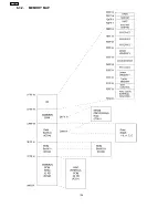
Страница 154: ...6 3 2 MEMORY MAP 126 KX FP101 ...
Страница 166: ...138 KX FP101 ...
Страница 176: ...6 4 6 3 2 Transmitting documents 6 4 6 3 3 Receiving FAX 148 KX FP101 ...
Страница 177: ...6 4 6 3 4 Copying 149 KX FP101 ...
Страница 188: ...b Redundancy Compression Process Coding Mode This unit uses one dimensional MH format 160 KX FP101 ...
Страница 212: ...12 1 MEMO KX FP101 184 ...
Страница 214: ...13 1 MEMO KX FP101 186 ...
Страница 216: ...14 1 MEMO KX FP101 188 ...
Страница 218: ...15 1 MEMO KX FP101 190 ...
Страница 220: ...16 1 MEMO KX FP101 192 ...
Страница 221: ...17 TERMINAL GUIDE OF THE IC S TRANSISTORS AND DIODES 193 KX FP101 ...
Страница 222: ...18 FIXTURES AND TOOLS 194 KX FP101 ...
Страница 223: ...19 CABINET MECHANICAL AND ELECTRICAL PARTS LOCATION 19 1 OPERATION PANEL SECTION 195 KX FP101 ...
Страница 224: ...19 2 UPPER CABINET SECTION 196 KX FP101 ...
Страница 225: ...19 2 1 PICK UP BASE SECTION 197 KX FP101 ...
Страница 226: ...19 3 LOWER P C B SECTION 198 KX FP101 ...
Страница 227: ...19 4 MOTOR SECTION 199 KX FP101 ...
Страница 228: ...19 5 ACTUAL SIZE OF SCREWS AND WASHER 200 KX FP101 ...
Страница 229: ...20 ACCESSORIES AND PACKING MATERIALS 201 KX FP101 ...
Страница 238: ...210 KX FP101 D Q KXFP101 Printed in Japan ...


