Operation manual for Narrow-pitch connectors F4S
Panasonic Corporation
industrial.panasonic.com/ac/e/
©
Panasonic Corporation 2017
ACCTF5E-5 201704
- 6 -
02-2. Precautions for board design
1) Circuit design
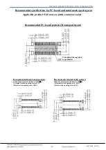
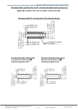
(1)When designing the terminal foot pattern, check the latest specifications and
examine the recommended foot pattern and dimensions of the metal mask opening.
The current recommendations are indicated on pages
13 and 14
.
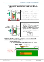
(2)This connector is provided with soldering metals for preventing solder from
peeling off the terminal.
Make sure to design a foot pattern for the holding metal.
(3)
Foot pattern layout considering mountability
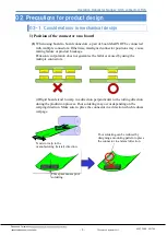
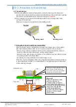
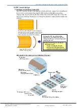
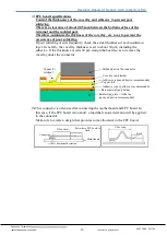
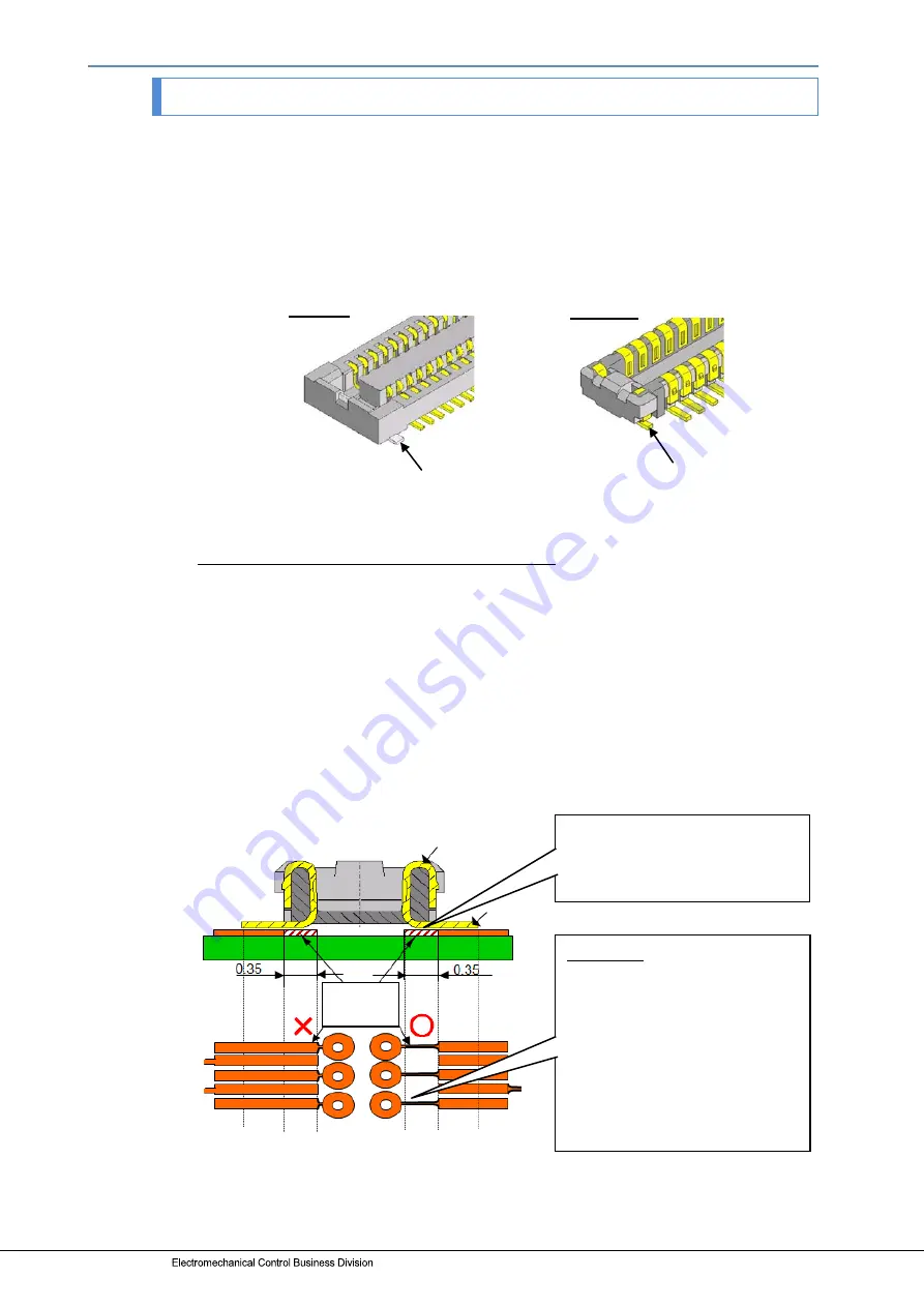
Since the header post is configured to extend to the bottom face of the molded
part, the following defects may occur if a pattern extends to the same area.
- When a large volume of solder is built up in the terminal back-fillet, solder is
likely to creep onto the molded part, causing solder bridges.
(Reason: Since slim designs are preferred, it is difficult to secure sufficient space
for pooling solder in the back-fillet.)
- Reworking becomes problematic if solder bridges occur.
Therefore, to prevent further solder creep, the terminal pattern is designed only up
to the molded part in MEW’s recommended PC-board pattern upon confirmation
of the soldering strength.
Holding metal
Socket
Header
Holding metal
This space is small, and thus when a
large volume of solder builds up
here, solder creeps onto the molded
part and causes solder bridges.
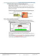
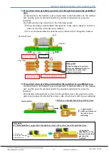
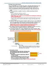
●
Key point
When a through-hole is made
under the connector, we
recommend that you thin the
pattern inside the prohibited area
as shown in the left-hand drawing
and provide a through-hole
outside the prohibited area.
In general, the pattern width in
this area is 1/3 the terminal
pattern width.
Sectional view
Top view
Through-hole
prohibited
area
post
terminal


