background image


Operation manual for Narrow-pitch connectors F4S 


Panasonic Corporation
industrial.panasonic.com/ac/e/ 


©

 Panasonic Corporation 2017 

ACCTF5E-5   201704 


- 3 -


02. Precautions for product design 

02-1. Considerations in mechanical design 

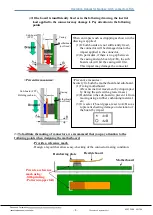
1) Position of the connector on a board  


(1) 

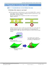
When using board to board connectors, a pair of board shall NOT be connected   

with multiple connectors. Otherwise, misaligned connector positions may  cause   
mating failure or product breakage. 
Panasonic corporation does not guarantee the failures caused by using the 
multiple connectors. 


(2)Rigid boards tend to warp in a direction perpendicular to the rolling direction 
during the production process. Poor soldering may occur depending on the 
warping direction. Make sure to place the connector in a direction which reduces 
warpage. 


This space causes poor  
soldering.  


Tends to warp in the 
 manufacturing (lateral) direction.  

Poor soldering can be reduced by  
designing a mounting pattern to place  
the connector in a lateral direction.  


×

Содержание F4S

Страница 1: ...ACCTF5E 5 2017 04 industrial panasonic com ac e F4S Narrow pitch Connectors Operation manual ...

Страница 2: ... ACCTF5E 5 201704 1 Contents 01 Introduction 2 02 Precautions for product design 3 03 Precautions for mounting and reflow soldering 15 04 Precautions for mating and unmating 21 05 Connectors for inspection and precautions for use 24 Points which particularly need to be confirmed before designing products are bold and underlined ...

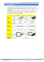
Страница 3: ...d part has been further reduced Select the types best suited to the conditions of use Read this document before designing a product and starting production F4S F4 Space saving Excellent Very good Width 3 6mm Width 5 0mm Wiring underneath Good Exposed metal part Excellent No exposed metal part Exposed metal part on the rear face Contact reliability Excellent Excellent Drop resistance Very good Bell...

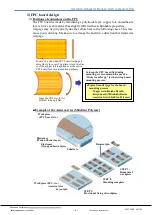
Страница 4: ...ector positions may cause mating failure or product breakage Panasonic corporation does not guarantee the failures caused by using the multiple connectors 2 Rigid boards tend to warp in a direction perpendicular to the rolling direction during the production process Poor soldering may occur depending on the warping direction Make sure to place the connector in a direction which reduces warpage Thi...

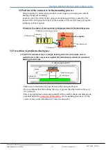
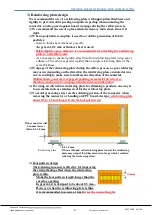
Страница 5: ...revention of problems during use 1 The F4S connectors have a simple locking structure but make sure to consider preventive measures against the detachment of mated connectors during practical use Make sure to eliminate any gaps between the casing and board We recommend that the holding force is set greater than the insertion force of the connector Select an appropriate cushioning material with a s...

Страница 6: ...onnector will be damaged due to the impact applied to the connector 2 In particular if there is no gap between the casing and sub board A B the sub board side will hit the casing wall first This impact may damage the connector Preventive measures Securely fix both the motherboard and sub board 1 Fixing motherboard Prevents inertial movement by drop impact by fixing the side with a greater mass 2 H...

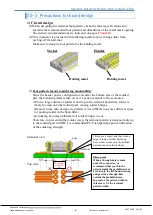
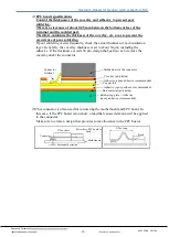
Страница 7: ...der is built up in the terminal back fillet solder is likely to creep onto the molded part causing solder bridges Reason Since slim designs are preferred it is difficult to secure sufficient space for pooling solder in the back fillet Reworking becomes problematic if solder bridges occur Therefore to prevent further solder creep the terminal pattern is designed only up to the molded part in MEW s ...

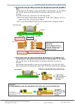
Страница 8: ...extends down to the bottomface of the molded part and the post extends horizontally beyond the molded part becomes the terminal If an insulated through hole is placed in the prohibited area the gap between the pattern and connector terminal becomes wider which may result in poor soldering interfering with adjacent terminal interfering with adjacent terminal Lead out straight to avoid interference ...

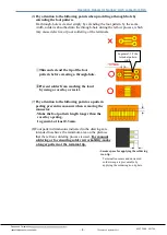
Страница 9: ...a through hole Prevent solder from reaching the land by using a coverlay or resist 7 Pay attention to the following point as a pattern peeling preventive measure when removing the connector Make the foot pattern length longer than the coverlay opening In general at least 0 3 mm 8 Foot pattern dimensions indicated in the drawings are intended to achieve the minimum area on the premise that the refl...

Страница 10: ...nEtsu Polymer In case of a one sided FPC board warpage is more likely to occur if a pattern is laid in a line or if the copper foil is applied over the entire FPC board for noise prevention purposes Since the FPC is soft it is difficult to keep it flat Typical transfer jigs for the board mounting process Magic resin Daisho Denshi Keiju board Mitsubishi Resin Assist carrier ShinEtsu Polymer To keep...

Страница 11: ...ly the coverlay thickness is set to about 30 μm including the adhesive If the thickness exceeds 30 μm design the board so as to remove the coverlay under the connector 3 This connector is often used for connecting the motherboard and FPC board In this case if the FPC board is too short a load that causes deviation will be applied to the connector Make sure to create a design that provides some all...

Страница 12: ...y occur depending on the direction the reinforcing plate on material was cut Accordingly make sure to indicate the direction of the material Rolled sheets generate warpage depending on material direction so therefore make sure to warpage reduction into consideration 4 For using an ultra thin reinforcing plate for slimming a product one way is to use metals such as stainless steel for the reinforci...

Страница 13: ...g the finish quality in a test run 2 Compared with natural air reflow soldering N2 reflow soldering can reduce oxidization of the melted solder surface This significantly improves the solder wettability Therefore make sure to apply an appropriate amount of solder 3 Do not apply an excessive amount of solder otherwise solder or flux may creep near the contact section and reduce contact reliability ...

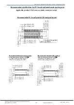
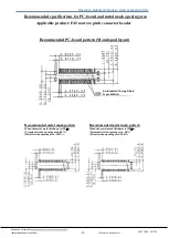
Страница 14: ...area Applicable product F4S narrow pitch connector socket Recommended PC board pattern Mount pad layout Uninsulated through hole is prohibited Recommended metal mask pattern When the metal mask thickness is 120 µm Terminal section opening area 60 Metal section opening area 100 Recommended metal mask pattern When the metal mask thickness is 150 µm Terminal section opening area 48 Metal section open...

Страница 15: ...area Applicable product F4S narrow pitch connector header Recommended PC board pattern Mount pad layout Uninsulated through hole is prohibited Recommended metal mask pattern When the metal mask thickness is 120 µm Terminal section opening area 60 Metal section opening area 100 Recommended metal mask pattern When the metal mask thickness is 150 µm Terminal section opening area 48 Metal section open...

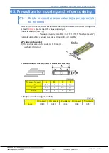
Страница 16: ...rce at least 10 times greater than the connector weight Theoretical lifting force g Vacuum pressure mmHG 760 1 033 Nozzle area cm2 Example of machine vacuum pressure setting 480 520 mmHg Picking up the socket 1 The suction area on the socket is 0 8 mm in the shorter direction Example of the nozzle Source Panasonic Factory Number of contacts A B C D 10 1 4 1 1 0 5 20 30 3 9 1 2 4 0 5 40 50 8 1 6 0 ...

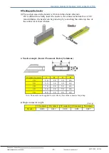
Страница 17: ...ace of 0 8 mm widthwise the header can be picked up by converting the entire top face of the connector as shown below Nozzle example Source Panasonic Factory Solutions Number of contacts A B C D 10 3 0 1 8 1 0 0 6 20 5 0 1 8 3 0 0 6 30 7 0 1 8 5 0 0 6 40 9 0 1 8 7 0 0 6 50 11 0 1 8 9 0 0 6 Single connector weight 10 contacts 20 contacts 30 contacts 40 contacts 50 contacts Header 0 008 0 013 0 018 ...

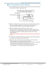
Страница 18: ...on then excessive solder may have been applied or the wicking phenomenon may have occurred Check the amount of solder applied the position and the temperature profile at the mounted connector position In particular be careful not to apply excessive solder when the N2 reflow furnace is used 4 Extending the screen pattern outward and providing a solder application position on the outer side can help...

Страница 19: ... 2 During solder rework solder is supplied at and the soldering iron is applied to the tip of each pattern Make sure that solder and the soldering iron do not contact the terminal 3 When carrying out manual soldering or rework avoid using flux if possible in order to prevent it from rising to the contact section For details see the next page 4 When using flux apply as little as possible to the tip...

Страница 20: ... Bonkote 2 Selection of soldering iron For narrow pitch connectors with a 0 4 mm pitch we recommend An iron tip with a retractable knife shape Ex Japan Bonkote With a temperature sensor on the iron tip Temperature controllable iron tip It is also necessary to check that there are no differences between the indicated temperature and the actual temperature of the iron tip The following temperatures ...

Страница 21: ...or 2 seconds Connector s resistance to soldering heat 300 C 5 sec max 350 C 3 sec max Thin wire solder with a diameter of 0 3 0 4 mm is recommended Final soldering is recommended after provisionally soldering the terminals at both ends Note that when the soldering iron touches the terminal wicking or contact failure may occur 2 Detailed precautions on how to apply the iron tip 3 Flux cleaning meth...

Страница 22: ... the connector until mating between the simple locking sections and mating between the contacts and posts of both connectors are completed A snapping sound will indicate that the simple locking sections are completely mated 4 After completing the mating process check that the clearance between the FPC board and the motherboard is visibly even in both the X and Y directions If the space is not even...

Страница 23: ...the method of unmating described above is not feasible due to a lack of space around the connector try the following methods If the number of contacts is small lift around one of the shorter sides of the connector to unmate it If the number of contacts is large e g 50 contacts or more lift around one of the longer sides of the connector and then lift around the other longer side to unmate Avoid co...

Страница 24: ...nasonic Corporation 2017 ACCTF5E 5 201704 23 Proposal on unmating jig How to unmate 1 Hook the unmating jig onto one of the shorter side faces of the connector 2 Lift up the jig to unmate one side 3 Remove entirely by hand Detailed drawing of the unmating jig edge Tolerance unless otherwise specified 0 1 ...

Страница 25: ...ctors F4S Panasonic Corporation industrial panasonic com ac e Panasonic Corporation 2017 ACCTF5E 5 201704 24 05 Connectors for inspection and precautions for use The connector for inspection is in preparation Consult us if you are interested ...

Страница 26: ...orporation 2017 ACCTF5E 5 201704 25 Amendment history Manual No Date Changes ACCTF5E 1 October 2013 Company name and format change ACCTF5E 2 June 2015 Division name change ACCTF5E 3 December 2015 The temperature profile of reflow soldering changed ACCTF5E 4 March 2016 Revised P 3 ACCTF5E 5 April 2017 Revised P 3 ...

Страница 27: ...ACCTF5E 5 201704 2017 ...

Отзывы: