background image

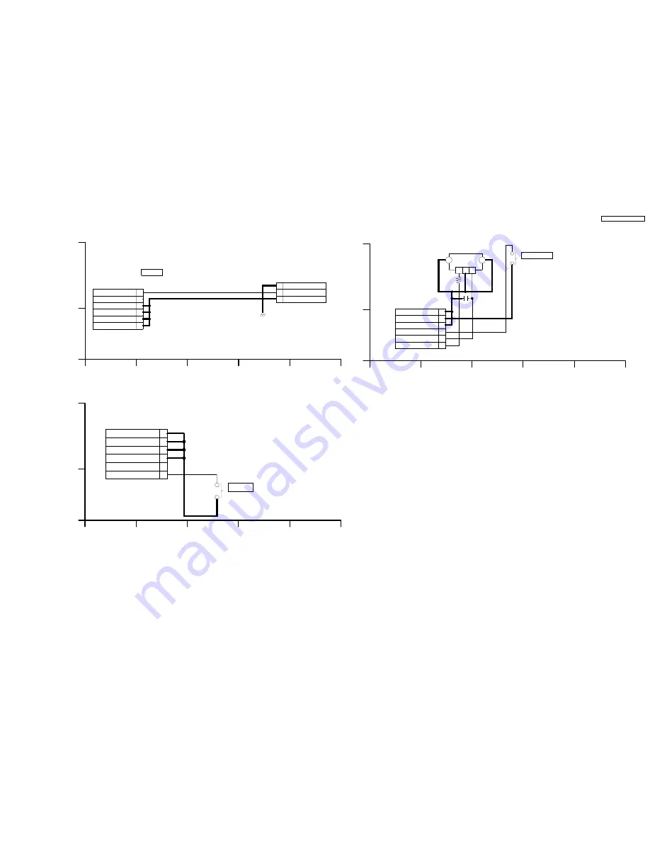
12.11. SW Schematic Diagram

1

3

2

JW7001

MAIN P.C.B.
(TIMER SECTION)

TO JW7501

2

4

3

1

6

5

K1KB06B00033

P7001

FRONT (L) P.C.B.

TO PP7701

GND

GND

KEY_POWER

GND

NC

GND

GND

GND

KEY_POWER

POWER

5

4

3

2

1

B

A

NOTE:DO NOT USE THE PART NUMBER SHOWN ON THIS DRAWING FOR ORDERRING.
           THE CORRECT PART NUMBER IS SHOWN  IN THE PARTS LIST,AND MAY BE
           SLIGHTLYDIFFERNT OR AMENDED SINCE THIS DRAWING WAS PREPARED.

DMR-EZ28P/PC
SW

Schematic Diagram

12.12. Front (L) Schematic Diagram

S7701

EVQ11G07K

2

4

3

1

6

5

K1KA06B00150

PP7701

SW P.C.B.

TO P7001

NC

GND

GND

GND

GND

POWER

KEY_POWER

5

4

3

2

1

B

A

NOTE:DO NOT USE THE PART NUMBER SHOWN ON THIS DRAWING FOR ORDERRING.
           THE CORRECT PART NUMBER IS SHOWN  IN THE PARTS LIST,AND MAY BE
           SLIGHTLYDIFFERNT OR AMENDED SINCE THIS DRAWING WAS PREPARED.

DMR-EZ28P/PC
Front (L)
Schematic Diagram

12.13. Front (R) Schematic Diagram

220

R7703

C7701

0.1

S7201

EVQ11G07K

RET2

RET1

G2

2

1

3

G1

PNA4618M13VT

IC7701

2

4

3

1

6

5

K1KA06B00150

PP7201

TO P7502

(Timer Section)

MAIN P.C.B.

IR

AD5V

GND

OPEN/CLOSE

GND

GND

KEY OPEN_CLOSE

5

4

3

2

1

B

A

NOTE:DO NOT USE THE PART NUMBER SHOWN ON THIS DRAWING FOR ORDERRING.
           THE CORRECT PART NUMBER IS SHOWN  IN THE PARTS LIST,AND MAY BE
           SLIGHTLYDIFFERNT OR AMENDED SINCE THIS DRAWING WAS PREPARED.

DMR-EZ28P/PC
Front (R)
Schematic Diagram

DMR-EZ28P / DMR-EZ28PC

55

Содержание DMR-EZ28P

Страница 1: ...tsushita Electric Industrial Co Ltd All rights reserved Unauthorized copying and distribution is a violation of law Model No DMR EZ28P DMR EZ28PC Vol 1 Colour K Black Type DVD Recorder ORDER NO CHM0802003CE B24 ...

Страница 2: ...on Specifications after Making Repairs 34 11 Block Diagram 35 11 1 Power Supply Block Diagram 35 11 2 Analog Video Block Diagram 37 11 3 Analog Audio Block Diagram 38 11 4 Analog Timer Block Diagram 39 12 Schematic Diagram 41 12 1 Interconnection Schematic Diagram 41 12 2 Power Supply Section Main P C B 1 4 Schematic Diagram A 42 12 3 AV IO 1 4 Section Main P C B 2 4 Schematic Diagram A 44 12 4 AV...

Страница 3: ... potential across the resistor 4 Check each exposed metallic part and measure the voltage at each point 5 Reverse the AC plug in the AC outlet and repeat each of the above measurements 6 The potential at any point should not exceed 0 75 volts RMS A leakage current tester Simpson Model 229 or equivalent may be used to make the hot checks leakage current must not exceed 1 2 milliampere In case a mea...

Страница 4: ...ly 3 Use only a grounded tip soldering iron to solder or unsolder ES devices 4 Use only an anti static solder removal device Some solder removal devices not classified as anti static ESD protected can generate electrical charge sufficient to damage ES devices 5 Do not use freon propelled chemicals These can generate electrical charges sufficient to damage ES devices 6 Do not remove a replacement E...

Страница 5: ...2 2 Precaution of Laser Diode 5 DMR EZ28P DMR EZ28PC ...

Страница 6: ... Solder PbF The lead free solder has to be used when repairing the equipment for which the lead free solder is used Definition The letter of PbF is printed on the PCB using the lead free solder To put lead free solder it should be well molten and mixed with the original lead free solder Remove the remaining lead free solder on the PCB cleanly for soldering of the new IC Since the melting point of ...

Страница 7: ...3 Service Navigation 3 1 Service Information 3 2 Caution for DivX 7 DMR EZ28P DMR EZ28PC ...

Страница 8: ...4 Specifications 8 DMR EZ28P DMR EZ28PC ...

Страница 9: ...9 DMR EZ28P DMR EZ28PC ...

Страница 10: ...5 Location of Controls and Components 10 DMR EZ28P DMR EZ28PC ...

Страница 11: ...11 DMR EZ28P DMR EZ28PC ...

Страница 12: ...ed off 1 Turn off the power and press STOP CH UP keys on the front panel simultaneously for 5 seconds 6 1 1 2 When the power can not be turned off 1 Press POWER key on the front panel for over 10 seconds to turn off the power forcibly and press STOP CH UP keys on the front panel simultaneously for 5 seconds 6 1 2 When the Forcible Disc Eject can not be done 12 DMR EZ28P DMR EZ28PC ...

Страница 13: ...ct Pin JZJ0484 or minus screw driver small in the direction of arrow to eject tray slightly 6 Put deck upward and push out Tray by Eject Pin JZS0484 or minus screw driver small 7 It is necessory to paste the Sheet again after ejection of the disc Refer to the illustration of the Step 4 and below figure about the portion of pasting the Sheet 13 DMR EZ28P DMR EZ28PC ...

Страница 14: ...Note Use the replacement parts RMV0335 when the Sheet has not being stickability 14 DMR EZ28P DMR EZ28PC ...

Страница 15: ... display U72 HDMI connection error communication error This error is displayed when there are any communication problems with the unit and the equipments TV amplifier etc connected to the unit by HDMI or when there is a problem with the HDMI cable U72 display disappears when error has been solved by Power OFF ON of connecting equipment or by inserting removing of HDMI cable U73 HDMI connection err...

Страница 16: ...supported format disc was played although the drive starts normally The data format is not supported although the media type is supported Exceptionally in case of the disc is dirty This disc is incompatible Display for 5 seconds NO READ Disc read error A disc is flawed or dirty A poor quality failed to start The track information could not be read Cannot read Please check the disc HARD ERR Drive e...

Страница 17: ...Lock is being set this Forced disc eject function is not accepted The display before execution leaves When the power is off press STOP and CH UP keys simultaneously for 5 seconds Forced power off When the power button is not effective while power is ON turn off the power forcibly When Schedule Recording is ON execute Forced Power off after releasing Schedule Recording Display in P off mode Press P...

Страница 18: ...keys simultaneously for 5 seconds When unlock the tray UNLOCK is displayed for 3 seconds When the power is on press STOP and POWER keys simultaneously for 5 seconds When press OPEN CLOSE key while the tray being locked Display LOCK for 3 seconds Press OPEN CLOSE key while the tray being locked ATP Initialization ATP setting and all parameters including clock are initialized and the unit turns off ...

Страница 19: ... Description Front Key Progressive initialization The progressive setting is initialized to Interlace The display before execution leaves When the power is on E E mode press STOP and PLAY simultaneously for 5 seconds 19 DMR EZ28P DMR EZ28PC ...

Страница 20: ...ut from AV Decoder Magenta picture Saturation rate 100 It is enable to switch Interlace Progressive by I P switch 1 4 Initial mode is Interlace Press 1 2 in service mode Switch Interlace Progressive Press 1 4 in Magenta Picture Output mode I P are switched alternately I P Switch Switch Interlace and Progressive in EE mode Initial setting is Interlace This command is effective during executing Whit...

Страница 21: ... Check laser used time hours of drive O is the used time display in hour OLaser used time of DVD CD in Playback Recording mode is counted Press 4 1 in service mode Delete the Laser Used Time Laser used time stored in the memory of the unit is deleted Press 9 5 in service mode 21 DMR EZ28P DMR EZ28PC ...

Страница 22: ...econds 5 Last Drive Error code No 2 1 2 is displayed for 5 seconds This Error Code is unnecessary for service 6 Last Drive Error code No 2 2 2 is displayed for 5 seconds This Error Code is unnecessary for service 7 Error occurring Disc type is displayed for 5 seconds DISC 1 DVD DISC 2 CD DISC 3 DVD RAM 2 6GB DISC 4 DVD RAM 4 7GB DISC 5 DVD R DISC Unknown Disc 8 Unused No display 9 Factor of Drive ...

Страница 23: ...ma signal and check the output on the S terminal Press 5 2 in service mode S2 signal output Forcibly superimpose the S2 signal approx 2V DC on the EE chroma signal and check the output on the S terminal Press 5 3 in service mode Front connection inspection Press all front keys and check the connection between Main P C B and Front key Switches 1 Each time a key is pressed segment turned on increase...

Страница 24: ...ating unit Second Press 6 5 in service mode Then press 0 1 1 9 the past 19 error histories are displayed Delete the Error History Delete Error History information stored on the unit Press 9 7 in service mode Tray OPEN CLOSE Test The RAM drive tray is opened and closed repeatedly Press 9 1 in service mode When releasing this mode press the POWER button of Remote Controller more than 10 seconds Erro...

Страница 25: ...Fan Motor Main P C B 3 Pin Same as ES15 EH55 Series JZS0484 Eject Pin Same as EH55 EH75V ES35V Series RFKZ03D01K Lead Free Solder 0 3mm 100g Reel Same as EH55 EH75V ES35V Series RFKZ06D01K Lead Free Solder 0 6mm 100g Reel Same as EH55 EH75V ES35V Series RFKZ10D01K Lead Free Solder 1 0mm 100g Reel Same as EH55 EH75V ES35V Series RFKZ0316 Solder Remover Lead free low temperature Solder 50g Same as E...

Страница 26: ... Chart The following chart is the procedure for disassembling the casing and inside parts for internal inspection when carrying out the servicing To assemble the unit reverse the steps shown in the chart below 9 2 P C B Positions 26 DMR EZ28P DMR EZ28PC ...

Страница 27: ... R P C B and Front L P C B 1 Unlock 6 tabs in A F turn Pull with the front panel in the direction of your side 2 Remove the 2 screws to remove Front R P C B and Front L P C B 9 4 1 How to assemble Tray door ass y 1 Attach Blinder spring to Tray door ass y 2 Attach Tray door ass y in order from to Put the Brinder spring on the groove Insert the shaft in the hole Insert the shaft in the hole 27 DMR ...

Страница 28: ...e and FFC to remove DV jack P C B and SD USB P C B CAUTION When replacing Digital P C B pay attention as below 9 6 Rear Panel 1 Remove 6 Screws A and 2 Screws B 2 Unlock 2 Locking Tabs A to remove Rear Panel 9 6 1 Only Fan Motor 1 Remove the 2 Screws C and connector remove the Fan motor 28 DMR EZ28P DMR EZ28PC ...

Страница 29: ... remove Digital P C B CAUTION When replacing Digital P C B pay attention as below 9 8 DVD Drive 1 Remove 3 Screws A and wire with connector to remove DVD Drive Caution when assembling DVD drive When assembling DVD drive draw around wire with connector between capacitors on Main P C B as following 29 DMR EZ28P DMR EZ28PC ...

Страница 30: ...9 9 Main P C B and SW P C B 1 Remove SW P C B 2 Remove 2 Screws A to remove Front angle 3 Remove Side angle Remove 4 Screws A and Rear angle to remove Main P C B 30 DMR EZ28P DMR EZ28PC ...

Страница 31: ...10 Measurements and Adjustments 10 1 Service Positions Note For description of the disassembling procedure see the section 9 10 1 1 Checking and Repairing Digital P C B 31 DMR EZ28P DMR EZ28PC ...

Страница 32: ...10 1 2 Checking and Repairing of Main P C B 32 DMR EZ28P DMR EZ28PC ...

Страница 33: ... replacing Digital P C B TM L1 is displayed after replacing Digital P C B Once power off and start up again 10 3 Caution for Replacing Parts 10 3 1 Items that should be done after replacing parts 33 DMR EZ28P DMR EZ28PC ...

Страница 34: ...t to establish the judgement criteria for the picture and sound Item Contents Check Item Contents Check Picture Block noise Sound Distorted sound Crosscut noise Noise static background noise etc Dot noise The sound level is too low Picture disruption The sound level is too high Not bright enough The sound level changes Too bright Flickering color Color fading 34 DMR EZ28P DMR EZ28PC ...

Страница 35: ...1 L1101 ABSORBER SURGE AND SUPPRESSOR SURGE F1101 P1101 AC SOCKET DMR EZ28P PC Power Supply Block Diagram H H ON REG ANA 3 3V ANA 3 3V 8 5 1 VIN VOUT IC1320 IC7501 3 CONT VC 1 VIN IC1330 5 REG X SW 5 2V X SW 5 2V E VOUT D5V P ON 7 IC7501 98 7 POWER TRANS T7501 1 REG D 5V IC1340 2 1 4 VIN VOUT Timer Section D 5V UNREG38V X SW 12V X SW 12V DR 5V IC7591 8 P SAVE L IC7501 75 F X SW 5 8V H DI P ON DL2 ...

Страница 36: ... 3V 29 P7401 P55201 E 1 P7401 P55201 35 37 P7401 P55201 D 5V D 5V 11 13 P7401 P55201 X SW 12V X SW 12V I UNREG38V 39 P55201 P7401 3 P55201 P7401 32 AU 5V X SW 5 2V P55201 P7401 17 SW 5V P55201 P7401 21 P55201 P7401 C X SW 5 8V X SW 5 8V 1 2 DR 12V P1240 47 X SW 4V P55201 P7401 23 25 D 3 3V P55201 P7401 43 T 1 5V P55201 P7401 4 DR 5V DR 5V P1240 3 4 S D D G D D 2 5 1 6 Q1250 REG X SW 4V 7 1 VIN CS ...

Страница 37: ...3002 FRONT S VIDEO IN JACK JK3004 4 IN S VIDEO 6 3 14 VIDEO IN JACK A V IN JK3001 FROM DIGITAL BLOCK SECTION FROM TO DIGITAL BLOCK SECTION P7401 P55201 P55201 P7401 P7401 P55201 P7401 P55201 P7401 P55201 RPROUT DM BPYOUT DM GPYOUT DM YOUT DM COUT DM D L3 OUT D L2 OUT D L1 OUT 79 77 Y V INTERFACE IIC BUS V SW Y SW C SW Y SW C SW V SW CLAMP CLAMP CLAMP CLAMP CLAMP IIC DATA IIC CLOCK 8 C1 S1 S2 DET 4...

Страница 38: ...ICAL 1 DIGITAL AUDIO OUT IC4901 SECTION DIGITAL BLOCK FROM 16 P55201 P7401 IECOUT LOUTL LOUTR 16 19 AUDIO L R 22 P55201 P7401 MIXROUT DM 20 P55201 P7401 MIXLOUT DM 100 XTMUTE Q4001 MUTE MUTE Q4002 QR4001 4002 4003 MUTE 36 P55201 P7401 XDMUTE AUDIO PROCESSOR SDA SCL L2 R IN L2 L IN L1 R IN L1 L IN TUN R IN TUN L IN 76 74 80 78 22 23 6 AUDIO L R FRONT R IN FRONT A V IN JACK JK3002 4 7 FRONT L IN R I...

Страница 39: ...R MAIN CLK 10MHz X7501 X SW 12V DI P ON D5V P ON H H DR P ON 71 DR P ON BLOCK SECTION FROM VIDEO XT MUTE HDMI P ON H BLOCK SECTION POWER TO S1 S18 G1 G4 S7201 CLOSE OPEN S7504 RESET SENSOR REMOTE CTL REC S7501 S7503 STOP CH DOWN S7506 1 2 P7502 P77201 3 FRONT R P C B P7502 P77201 P7502 P77201 IC7701 Q7502 CONTROL P SAVE QR7503 P SAVE L OFF HDMI IN 28 P7401 P55201 5 HDMI MONI XINTM 27 P7401 P55201 ...

Страница 40: ...DMR EZ28P DMR EZ28PC 40 ...

Страница 41: ...PNCIN DM DGND AU5V DGND AUGND ANA3R3V AADC_L DGND AADC_R D3R3V AUGND D3R3V MIXROUT DM X SW 6V MIXLOUT DM UART2 TX AUGND SW5V IECOUT UART2 RX XFWE D5V XMPREQ D5V SBPTM HDMI P5 ON H XINTP HDMI CONT SBMTP HDMI MONI XINTM DI PON DL H SCLK DI PON H P7401 P1240 64 63 62 61 60 59 58 57 56 55 54 53 52 51 50 49 48 47 46 45 44 43 42 41 40 39 38 37 36 35 34 33 32 31 30 29 28 27 26 25 24 23 22 21 20 19 18 17 ...

Страница 42: ... 0 4 2 1 3 5 IC1340 C0DAEYH00002 C1252 0 1 R1200 22K D L1250 G0A100HA0023 C1250 25V220 C1251 1 C1254 27P C1253 0 1 R1251 33K CL1203 R1261 68K D R1260 3600 D R1252 27 10V100 C1263 4 2 1 3 5 C0DBEKG00003 IC1260 1 2 5 6 3 4 B1DHDD000022 Q1250 820 D R1253 K1250 VWJ0795 5 G0A100K00003 L1251 4 2 1 3 5 C0DAEYH00002 IC1360 J0JHC0000048 LB1250 C1231 10V680 L1230 G0A100H00025 R1206 2400 D R1203 5600 D 0 047...

Страница 43: ...N SHUTDOWN THERMAL LIMITTER CURRENT DRIVER BIAS REFERENCE 7 1 3 2 4 5 6 Vc Vout 1 4 Sense 5 GND 3 2 Vin REF TSD Vc Vout 1 4 ADJ 5 GND 3 2 Vin REF TSD ON OFF OCP Drive AMP1 IC1120 Detail Block Diagram IC1250 Detail Block Diagram IC1260 Detail Block Diagram IC1320 Detail Block Diagram IC1330 Detail Block Diagram IC1340 Detail Block Diagram IC1350 Detail Block Diagram IC1360 Detail Block Diagram DMR ...

Страница 44: ... 15K 25V47 25V47 C4012 8 2K 8 2K R4017 C4010 1000P 100P C4009 820 820 R4014 CL7464 CL7463 CL7461 GND 100P C4008 Y_IN C_IN PY_IN T 5V_VCC 9V_VCC ALWAYS_5V C1_IN GND V2_IN VCR C Y1_IN C1_S1 S2_DET Y2_IN C2_IN C2_S1 S2_DET BAND_GAP VY_TO_DVD C_TO_DVD SLICER_OUT SYNC_SEPA 21 V1_OUT 80 L1 R_IN RF_A_OUT AR_TO_DVD AL_TO_DVD 64 9V 2_VCC 78 L1 L_IN AL_FROM_DVD D_L2_OUT AR_FROM_DVD 62 A_OUT_L2 61 A_OUT_R2 6...

Страница 45: ...19B0004 K1U822B00003 CPN LINE OUT Y C C or or CPN LINE1_IN LINE1 IN R LINE1 IN V LINE1 IN L CY PY Cr Pr Cb Pb LINE OUT L LINE OUT R LINE OUT V Y B DMR EZ28P PC AV IO Section 2 4 Main P C B 2 4 Schematic Diagram A P Power Supply Section Page A A AV IO Section Page B TU Tuner Section Page T Timer Section Page C D NOTE DO NOT USE THE PART NUMBER SHOWN ON THIS DRAWING FOR ORDERRING THE CORRECT PART NU...

Страница 46: ...7 10K UNR521100L QR4003 UNR511100L QR4002 16V470 C4020 T TU TU LINE2 IN R LINE2 IN V LINE2 IN L VIN AU9V GND ON H VOUT NR UNR5211 TX C Y P T UNR5211 TX UNR5111 TX B DMR EZ28P PC AV IO Section 3 4 Main P C B 2 4 Schematic Diagram A P Power Supply Section Page A A AV IO Section Page B TU Tuner Section Page T Timer Section Page C D NOTE DO NOT USE THE PART NUMBER SHOWN ON THIS DRAWING FOR ORDERRING T...

Страница 47: ...VCC B DMR EZ28P PC AV IO Section 4 4 Main P C B 2 4 Schematic Diagram A P Power Supply Section Page A A AV IO Section Page B TU Tuner Section Page T Timer Section Page C D NOTE DO NOT USE THE PART NUMBER SHOWN ON THIS DRAWING FOR ORDERRING THE CORRECT PART NUMBER IS SHOWN IN THE PARTS LIST AND MAY BE SLIGHTLYDIFFERNT OR AMENDED SINCE THIS DRAWING WAS PREPARED 20 21 22 19 a b c d Z Y TO AV IO SECTI...

Страница 48: ...LPF Bias CL Bias CL Bias CL 40 45 43 29 32 30 28 Y2 OUT C2 OUT V2 OUT PY OUT 41 38 36 34 35 16 52 39 PB OUT PR OUT 75Ω 75Ω 75Ω 75Ω 75Ω 75Ω 17 VCC 55 50 37 27 L ch R ch 57 58 L CH R CH A OUT R2 A OUT L2 A OUT R2 A OUT L2 60 63 61 62 80 72 76 78 71 74 IC3001 VIDEO AUDIO PROCESSOR IC DETAIL BLOCK DIAGRAM IC3001 Detail Block Diagram IC4001 Detail Block Diagram IC4901 Detail Block Diagram DMR EZ28P PC ...

Страница 49: ...891 VWJ0795 7 5 G_TUIFOUT1_A G_TU_SDA_A AFC G_TU_SCL_A RFC_SW RFC_5V AUDIO_IN BOOSTER_5V TU_MONITOR NC SIF_OUT VIF_5V VIDEO_OUT AFT 30V TUNER_5V IFD_OUT2 IFD_OUT1 IF_OUT IF_AGC IIC_CLK IF_OUT_TW IIC_SDA VIDEO_IN AGC RFC_ON OFF A A P A A VO CN GND VIN PCTNWID DBXIN PCKE6B PCSPE SDA SCL PCDET PCTIM PCDCIN STPDET STPLL PCPLC GND POSIF PCFIL ROUT ADDSET ST_SAP PCREG LOUT VCC PCDCOUT SAPDET CONT A T A ...

Страница 50: ...PON_H D5V_PON_H FAN_PWM R7593 22K HDMI_MONI 100 R7547 XMPREQ_T 1K R7515 XINTP_T 79 77 76 78 49 47 48 50 74 71 72 67 68 56 55 58 57 52 51 54 53 65 66 61 62 59 60 64 63 70 69 73 75 10 8 7 9 12 11 99 100 95 94 96 97 90 91 89 93 92 98 4 6 5 2 1 3 81 82 80 86 87 88 84 83 85 45 19 17 15 14 16 18 43 23 21 20 22 41 24 39 37 33 35 34 29 29 PFAIL_L 30 27 26 28 32 31 36 38 25 40 42 44 13 46 IC7501 MN67789TA ...

Страница 51: ...ad Data Write Data Address Scan Pulse Timing Clock RAM Code CGRAM CGROM Circuit Control FL Decoder Command Code Generator Clock XOUT XIN 10 11 Interface Serial Driver Digit Driver Segmemt G1 44 S1 S18 TBUS TXD TBUS RXD TBUS CLK X_RESET KEY IN1 KEY IN2 G2 G3 G4 4 5 6 8 17 KEY IN3 18 RST KEY 37 16 45 46 47 75 48 65 L1 SWIDE 19 XT MUTE 100 71 JC P ON H 7 DIP ON H DR P ON H 23 P SAVE H P FAL L 29 IR R...

Страница 52: ...MAIN CPU 1 Section 1 4 DIGITAL P C B K1MN07AA0003 TPA TPA TPB TPB TPA GND GND TPB TPB GND TPA 5 4 3 2 1 B A NOTE DO NOT USE THE PART NUMBER SHOWN ON THIS DRAWING FOR ORDERRING THE CORRECT PART NUMBER IS SHOWN IN THE PARTS LIST AND MAY BE SLIGHTLYDIFFERNT OR AMENDED SINCE THIS DRAWING WAS PREPARED DV JACK DMR EZ28P PC Schematic Diagram DMR EZ28P DMR EZ28PC 52 ...

Страница 53: ... 14 11 1 4 2 3 6 5 128 31 29 23 26 27 24 25 18 19 17 22 20 21 28 30 32 33 IC66802 C1CB00002799 S_D S_D P_3R3 PO DGND 0 1 C66815 0 1 C66810 P_1R8 VSS VSS D GND GND D PO Cn Vo NC GND Vin Cont Sub D5V 3R3V GND CLK SF_D8 GR4_N SF_D2 USB2602 GR3_N SF_D0 CF_SA0 MS_BS MS_D1 SF_D1 GPIO6 RBIAS GPIO8 VDD33 DAT3 VDD33 VDD18 DAT2 FG GPIO2 GPIO7 GPIO1 2 PRTPWR2 1 PRTPWR_POL 95 GPIO14 94 GPIO13 GPIO12 96 GPIO15...

Страница 54: ... IC Detail Block Diagram Vout Cn Vin Cont GND Bias Driver Current Limitter Reference Thermal Shutdown 1 4 7 5 3 IC66801 REG P 3 3V IC DETAIL BLOCK DIAGRAM IC66803 REG VBUS IC DETAIL BLOCK DIAGRAM USBUP DP 111 USBDN DM4 12 USBDN DP4 13 SD DATA0 99 SD DATA1 98 SD DATA2 105 SD DATA3 104 USBUP DM 110 1 IC66802 USB HUB AND SD CARD READER WRITER IC DETAIL BLOCK DIAGRAM DMR EZ28P DMR EZ28PC 54 ...

Страница 55: ...R KEY_POWER 5 4 3 2 1 B A NOTE DO NOT USE THE PART NUMBER SHOWN ON THIS DRAWING FOR ORDERRING THE CORRECT PART NUMBER IS SHOWN IN THE PARTS LIST AND MAY BE SLIGHTLYDIFFERNT OR AMENDED SINCE THIS DRAWING WAS PREPARED DMR EZ28P PC Front L Schematic Diagram 12 13 Front R Schematic Diagram 220 R7703 C7701 0 1 S7201 EVQ11G07K RET2 RET1 G2 2 1 3 G1 PNA4618M13VT IC7701 2 4 3 1 6 5 K1KA06B00150 PP7201 TO ...

Страница 56: ...DMR EZ28P DMR EZ28PC 56 ...

Страница 57: ... Circuit Board 13 1 Main P C B 13 1 1 Main P C B 1 4 Section 1 A B C D 2 3 4 5 1 4 2 4 3 4 4 4 DMR EZ28P PC Main P C B VEP79179A EZ28P VEP79179B EZ28PC 1 4 Section Location Map FRONT REAR DMR EZ28P DMR EZ28PC 57 ...

Страница 58: ...13 1 2 Main P C B 2 4 Section HOT COLD 5 6 7 8 9 1 4 2 4 3 4 4 4 DMR EZ28P PC Main P C B VEP79179A EZ28P VEP79179B EZ28PC 2 4 Section Location Map FRONT REAR DMR EZ28P DMR EZ28PC 58 ...

Страница 59: ...13 1 3 Main P C B 3 4 Section C D E F Main P C B 1 4 2 4 3 4 4 4 DMR EZ28P PC Main P C B VEP79179A EZ28P VEP79179B EZ28PC 3 4 Section Location Map FRONT REAR DMR EZ28P DMR EZ28PC 59 ...

Страница 60: ...13 1 4 Main P C B 4 4 Section HOT COLD 1 4 2 4 3 4 4 4 DMR EZ28P PC Main P C B VEP79179A EZ28P VEP79179B EZ28PC 4 4 Section Location Map FRONT REAR DMR EZ28P DMR EZ28PC 60 ...

Страница 61: ...B3002 F 2 C1361 C 5 C4901 A 2 R1120 C 7 R4007 C 2 R7539 E 5 QR4001 F 3 JK3001 A 3 LB3003 F 2 C1362 C 5 C4902 A 2 R1121 C 7 R4008 C 2 R7540 F 5 QR4002 F 3 JK3002 F 3 LB3004 C 4 C1363 D 5 C7301 B 4 R1122 C 7 R4009 D 2 R7541 E 5 QR4003 F 3 JK3003 A 4 LB3005 A 3 C3003 C 3 C7302 B 3 R1123 C 7 R4010 D 2 R7542 E 5 QR7503 F 7 JK3004 F 2 LB3006 A 3 C3004 C 2 C7304 B 4 R1124 C 7 R4011 D 2 R7544 E 5 QR7801 E...

Страница 62: ...13 2 Front L P C B 1 A B C D 2 3 4 5 DMR EZ28P PC FRONT L P C B VEP73154A FRONT L P C B 13 3 Front R P C B 1 A B C D 2 3 4 5 DMR EZ28P PC FRONT R P C B VEP73156A FRONT R P C B DMR EZ28P DMR EZ28PC 62 ...

Страница 63: ...13 4 DV Jack P C B 1 A B C D 2 3 4 5 DMR EZ28P PC DV JACK P C B VEP73155A DV JACK P C B 13 5 SW P C B 1 A B C D 2 3 4 5 DMR EZ28P PC SW P C B VEP70216A SW P C B DMR EZ28P DMR EZ28PC 63 ...

Страница 64: ...13 6 SD USB P C B 1 A B C D 2 3 4 5 6 7 8 9 Foil Side DMR EZ28P PC SD USB P C B VEP73163A Component Side SD USB P C B DMR EZ28P DMR EZ28PC 64 ...

Страница 65: ... 2 3 0 1 8 5 1 8 0 1 2 3 4 1 8 0 Ref No MODE 21 22 23 24 25 26 27 28 29 30 31 32 33 34 35 36 37 38 39 40 REC 2 3 3 3 3 3 2 5 0 1 2 3 5 2 3 0 1 2 5 0 2 3 0 2 5 2 5 2 3 5 2 3 0 1 2 3 PLAY 2 3 3 3 3 3 2 5 0 1 2 3 5 2 3 0 1 2 5 0 2 3 0 2 5 2 5 2 3 5 2 3 0 1 2 3 STOP 2 3 3 3 3 3 2 5 0 1 2 3 5 2 3 0 1 2 5 0 2 3 0 2 5 2 5 2 3 5 2 3 0 1 2 3 Ref No MODE 41 42 43 44 45 46 47 48 49 50 51 52 53 54 55 56 57 58...

Страница 66: ...4 6 0 1 6 4 1 4 1 9 4 12 2 4 1 4 1 0 0 1 1 0 0 1 1 PLAY 5 6 4 6 0 1 6 4 1 4 1 9 4 12 2 4 1 4 1 0 0 1 1 0 0 1 1 STOP 5 6 4 6 0 1 6 4 1 4 1 9 4 12 2 4 1 4 1 0 0 1 1 0 0 1 1 Ref No MODE E C B E C B E C B E C B E C B REC 0 11 8 0 2 12 2 12 11 5 5 6 12 2 6 2 1 9 0 1 2 0 0 1 0 6 PLAY 0 11 8 0 2 12 2 12 11 5 5 6 12 2 6 2 1 9 0 1 2 0 0 1 0 6 STOP 0 11 8 0 2 12 2 12 11 5 5 6 12 2 6 2 1 9 0 1 2 0 0 1 0 6 Re...

Страница 67: ... 11 12 STOP 15Vp p 5 sec div IC1120 1 STOP 8 4Vp p 5 sec div IC1120 2 STOP 0 2Vp p 5 sec div P7401 58 54 REC PLAY 0 4Vp p 20 sec div JK3903 2 REC PLAY 1 0Vp p 20 sec div JK3903 4 REC PLAY 2 0Vp p 20 sec div JK3903 3 REC PLAY 1 0Vp p 20 sec div P7401 42 REC PLAY 0 6Vp p 20 sec div P7401 46 REC PLAY 1 0Vp p 20 sec div P7401 50 REC PLAY 1 0Vp p 20 sec div 67 DMR EZ28P DMR EZ28PC ...

Страница 68: ...RTH H HA0 UP HD0 UP HINT HRXW HOST ADDRESS HOST DATA HOST INTERRUPT HOST READ WRITE INITIAL LOGO ABBREVIATIONS I IECOUT IPFRAG IREF ISEL IEC958 FORMAT DATA OUTPUT INTERPOLATION FLAG I CURRENT REFERENCE INTERFACE MODE SELECT L LDON LPC LRCK LASER DIODE CONTROL LASER POWER CONTROL L CH R CH DISTINCTION CLOCK M MA0 UP MCK MCKI MCLK MDATA MDQ0 UP MDQM MLD MPEG MEMORY ADDRESS MEMORY CLOCK MEMORY CLOCK ...

Страница 69: ... BACK VOLTAGE REFERENCE SOURCE POWER SUPPLY VOLTAGE W WAIT WDCK WEH WSR BUS CYCLE WAIT WORD CLOCK WRITE ENABLE HIGH WORD SELECT RECEIVER X X XALE XAREQ XCDROM XCS XCSYNC XDS XHSYNCO XHINT XI XINT XMW XO XRE XSRMCE XSRMOE XSRMWE XVCS XVDS XVSYNCO X TAL X ADDRESS LATCH ENABLE X AUDIO DATA REQUEST X CD ROM CHIP SELECT X CHIP SELECT X COMPOSITE SYNC X DATA STROBE X HORIZONTAL SYNC OUTPUT XH INTERRUPT ...

Страница 70: ...15 Parts and Exploded Views 15 1 Exploded Views 15 1 1 Casing Parts Mechanism Section 70 DMR EZ28P DMR EZ28PC ...

Страница 71: ...15 1 2 Packing Accessories Section 71 DMR EZ28P DMR EZ28PC ...

Страница 72: ...1A105A028 10V 1U 1 C1351 F2A1A1010072 10V 100U 1 Ref No Part No Part Name Description Pcs Remarks C1353 ECJ1VB1H103K 50V 0 01U 1 C1361 F2A1A1010072 10V 100U 1 C1362 ECJ1VB1C333K 16V 0 033U 1 C1363 F2A1A1010072 10V 100U 1 C3003 F1H1C104A090 16V 0 1U 1 C3004 ECJ1VB1H103K 50V 0 01U 1 C3005 ECJ1VB0J105K 6 3V 1U 1 C3006 F2A1C100B110 16V 10P 1 C3007 F1H1C104A090 16V 0 1U 1 C3008 ECJ1VB0J105K 6 3V 1U 1 C...

Страница 73: ...00067 DIODE 1 D7507 B0AADM000003 DIODE 1 D7508 B0AADM000003 DIODE 1 D7510 B0JDCE000002 DIODE 1 D7511 MAZ4120NHF DIODE 1 D7512 B0BA03600021 DIODE 1 D7801 B0BA03000015 DIODE 1 DP7501 A2BD00000169 DISPLAY TUBE 1 Ref No Part No Part Name Description Pcs Remarks DZ1101 J0LV00000001 SERGE ABSORBER 1 PC DZ1101 J0LY00000045 SERGE ABSORBER 1 P F1101 K5D202BK0005 FUSE 1 FL7301 J0B4504AA026 FILTER 1 IC1120 C...

Страница 74: ...75 1 R3024 ERJ3GEYJ102V 1 10W 1K 1 Ref No Part No Part Name Description Pcs Remarks R4001 ERJ3GEYJ133V 1 10W 13K 1 R4002 ERJ3GEYJ133V 1 10W 13K 1 R4003 ERJ3GEYJ123V 1 10W 12K 1 R4004 ERJ3GEYJ123V 1 10W 12K 1 R4005 ERJ3GEYJ133V 1 10W 13K 1 R4006 ERJ3GEYJ133V 1 10W 13K 1 R4007 ERJ3GEYJ123V 1 10W 12K 1 R4008 ERJ3GEYJ123V 1 10W 12K 1 R4009 ERJ3GEYJ153V 1 10W 15K 1 R4010 ERJ3GEYJ153V 1 10W 15K 1 R4011 ...

Страница 75: ...9 ERJ3GEY0R00V 1 10W 0 1 W530 ERJ6GEY0R00V 1 8W 0 1 W531 ERJ6GEY0R00V 1 8W 0 1 W532 ERJ3GEY0R00V 1 10W 0 1 W533 ERJ3GEY0R00V 1 10W 0 1 Ref No Part No Part Name Description Pcs Remarks W534 ERJ3GEY0R00V 1 10W 0 1 W535 ERJ3GEY0R00V 1 10W 0 1 W536 ERJ3GEY0R00V 1 10W 0 1 W537 ERJ3GEY0R00V 1 10W 0 1 W538 ERJ3GEY0R00V 1 10W 0 1 W539 ERJ3GEY0R00V 1 10W 0 1 W540 ERJ3GEY0R00V 1 10W 0 1 W541 ERJ3GEY0R00V 1 ...

Страница 76: ...FRONT L P C B 1 RTL 4 VEP73155A DV JACK P C B 1 RTL 5 VEP73156A FRONT R P C B 1 RTL 6 VEP73163A SD USB P C B 1 RTL 7 L6FAJCAE0001 FAN MOTOR 1 8 RGR0364F A1 REAR PANEL 1 P 8 RGR0364F B1 REAR PANEL 1 PC 9 RHD30111 3 SCREW 13 10 RHD30119 L SCREW 10 11 RMA2048 1 SIDE ANGLE 1 Ref No Part No Part Name Description Pcs Remarks 12 RMA2049 REAR ANGLE 1 13 RMA2093 FRONT ANGLE 1 14 RMC0728 EARTH SPRING 2 15 R...

Отзывы: