background image

14      9710 VCA

000216

(  ) Locate a 10K ohm resistor (brown-black-orange) and bend

the leads at right angles to the part as if installing on a circuit
board but slip one lead through  J11-T and the other through
J12-T.  Position the resistor close to the lugs and bend the leads
back  to mechanically secure them then cut off the excess.
Do not solder these connections.  This is R117 in fig 3.

(  ) Locate the remaining 10k (orange-orange-brown) resistor

 and trim both leads off to 1/2". Connect one lead to J12-T (ns)
and the other to J10-X (s1).  This is R116.

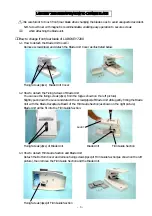
(  ) Locate the 91k  resistor (white-brown-orange) and extend

one lead with a 1" length of bare wire as shown.
Cut a 2-1/4" length of the large sleeving and slide it over
the resistor to make sure 1/4" or more of lead extends
from each end of the sleeving. If length is OK, remove the
sleeving and connect the extended lead to J12-T. Solder
the three wires at this connection. This is R115 in fig 3.

(  ) Slip the length of sleeving from above over R115 and connect

the free lead to J3-R. Bend back to secure Do not solder.

(  ) Locate the 47k resistor (yellow-violet-orange) and trim both

leads off to a length of 1/2". Slip one lead through J9-T and
solder this connection. This is R114.

(  ) Slip the free end of R114 through S2-2 and bend back to

secure. Do not solder this connection.

This completes the wiring between parts on the front panel.
Before going further, make sure that the bare wire is dressed
down against the panel and not in danger of shorting to unintended
solder lugs. Dress the insulated wires down also - they need not be
close to the panel but should not loop out away from the assembly.

A few connections will be made between the circuit board and
front panel before the two are fastened together. The figure that
illustrates the connection is shown to the right of the step.

FROM

TO

FROM

TO

(  ) "U"

R110-1 (s1)

Fig 4

(  ) "Z"

R112-1 (s1)

Fig 4

(  ) "F"

J10-T (s1)

Fig 4

(  ) "T"

J11-T (s2)

Fig 4

(  ) "I"

J13-T (s1)

Fig 5

2-1/4"

Twist leads

and solder

Содержание 9710

Страница 1: ...710 like a traditional VCA but with the added convenience of a built in Voltage Controlled Input Submixer and ADSR Envelope Generator This configuration of elements allows a couple of signals to be mi...

Страница 2: ...ay seem silly and ritualistic but it greatly decreases the chance of omitting a step and also provides some gratification and reward as each step is completed Numbered figures are printed in the Illus...

Страница 3: ...to cover the soldering pad and about 1 16 inch of lead passing through it There are two improper connections to beware of Using too little solder will sometimes result in a connection which appears to...

Страница 4: ...ends of each resistor in place as you install it Clip each lead flush with the solder joint and save a few of the clippings for use in later steps A tip If you can t find the location for a resistor...

Страница 5: ...37 R47 R60 R69 listed below 33 orange orange black R1 R2 R62 R68 R82 3300 orange orange red listed below 330k orange orange yellow R53 R55 R58 R83 R84 listed below 33k orange orange orange R51 R52 R70...

Страница 6: ...rts through the holes in the board and push the part against the circuit board as far as it wants to go Don t force it it s OK if it sits a little off the board Capacitors are often marked with obscur...

Страница 7: ...c kits may have a higher Voltage V rating than the minimum specified below DESIGNATION VALUE C20 10uF 15V C21 10uF 15V C16 1uF 15V C1 220uF 25V C2 220uF 25V C19 33uF 15V C4 4 7uF 15V C6 4 7uF 15V Diod...

Страница 8: ...ESIGNATION TYPE Q3 Q4 2N3904 NPN Si Transistor Matched Pair One transistor has been selected for use as a noise source and has one of its leads cut short Q5 2N3906 Selected for noise Install the remai...

Страница 9: ...formed into the case of the IC corresponding to pin 1 or a semicircular notch that indicates the end of the package with pin 1 Take care that this polarizing indicator corresponds to the similar indic...

Страница 10: ...re soldering the second lead and trimming both leads off flush with the solder joint DESIGNATION TYPE LED1 Red LED Flying Wires i e those which go from circuit board to panel mounted parts In the foll...

Страница 11: ...indicates a cold joint reheat them Solder bridges are less likely with a solder masked circuit board but they can still happen If you re not sure about a bridge refer to the foil patterns in fig 1 Fro...

Страница 12: ...rient the pots with the solder lugs as shown in fig 3 and fully tighten the nuts to secure them A tip marking the part number e g R109 on the back of the pots with an indelible pen will make later wir...

Страница 13: ...out 1 1 4 long extends beyond J9 Solder the connections to the S lugs of J1 and J9 first then bend the S lugs of J2 J8 up and solder them to the wire as was done on the previous jacks Connect the free...

Страница 14: ...he three wires at this connection This is R115 in fig 3 Slip the length of sleeving from above over R115 and connect the free lead to J3 R Bend back to secure Do not solder Locate the 47k resistor yel...

Страница 15: ...in the L brackets When satisfied with the alignment of panel LED and circuit board fully tighten the hardware Finish panel assembly by connecting the remaining wires from the circuit board to the jack...

Страница 16: ...inst the wire and pin until the solder remelts You should not need to add more solder Allow the joint to cool and test it by wiggling the wire to make sure the joint is firm Do not wrap the wings of t...

Страница 17: ...and start testing which makes this is an great time to take another break stretch and think about something else for a while When you come back take the time to do a final check The flying wires to t...

Страница 18: ...e g if when panning from L to R you hear the pitched source increase in volume but hear no noise it means that at least the R VCA is working OK But you can infer more than that since sections of all...

Страница 19: ...ng with the way J6 is wired 6 Switch the modulator from Cycle to ADSR and connect a gate source to Modulation input G Gate Gate signals should be true positive transition from ground to a positive vol...

Страница 20: ...at this input normals to the ADSR output You ll have to remember on your own that there s a 10dB V exponential converter as part of this connection External inputs interrupt the normal and the expo co...

Страница 21: ...ng the Attack phase Clockwise rotation of the control slows the rate which is variable from 500uS to as long as 10 seconds Decay control Sets the rate at which the ADSR function falls from the peak re...

Страница 22: ...t will at some point exceed the Sustain level and IC7 D will switch from low to high but this simply prepares the circuit for the Decay phase which will happen later and produces no effect at this tim...

Страница 23: ...the voltage on the wiper of the Pan control goes from 0 to 12V and increase the L gain IC3 B and associated components outputs a voltage that is the inverse of the Pan control setting for decreasing...

Страница 24: ...brown grey orange R71 R81 R85 R87 5 1k brown black red R25 R26 R80 R99 R107 5 220 red red brown R35 R36 R45 R46 R98 1 2200 red red red R20 6 220k red red yellow R16 R17 R75 R78 R88 R97 5 22k red red...

Отзывы: