5S-P-003
Program Writer
© Copyright 2022, PADAUK Technology Co. Ltd
Page 18 of 34
5S-P-003-UM-EN-V007
– Oct. 14, 2022
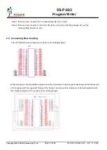
5. Connecting Board Making Description
JP7 can support various customizing package pin based on Connecting Board.
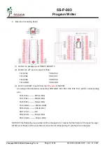
The making and rules of the Connecting Board as follows:
(1) Define the information of package pin in program.
(2) Make the Connecting Board.
(3) For developed PDK files, adding the information of package pin please refer to
section 5.5.
5.1. Define the data of exclusive use packaged pin
Define the data of exclusive use packaged pin in program. Here is grammar:
.writer package
….,
(A total of thirteen sets of values)
For example:
.writer package
16, 5, 11, 9, 10, 8, 7, 6, 14, 0x00F0, 0x00F4, 0, 0x04
Grammar instruction
Group
Count
Name
Introduction
Remarks
1
Pin
Count
(the number of pin)
Up to 28 pins
2
VDD
VDD pin number
3
PA0
PA0 pin number
Note 1
4
PA3
PA3 pin number
5
PA4
PA4 pin number
6
PA5
PA5pin number
7
PA6
PA6 pin number
8
PA7
PA7 pin number
Note 1
9
GND
GND pin number
10
Mask1
Package the left pin mask value, each bit
represents a pin
BIT0
1st pin, BIT2
2nd pin,
BITn (n=0..13) 0/1: bypass/ O/S test
Set 0:this pin not do O/S test
Set 1:this pin do O/S test
Note 2
11
Mask2
Package the right pin mask value, each
bit represents a pin;
BIT0
m pin, BIT2
(m-1)pin,
BITn (n=0..13) 0/1: bypass/ O/S test
Set 0:this pin not do O/S test
Set 1:this pin do O/S test
m: The number of pin
Note 2
12
Shift
IC is corresponding to the blank space
number need to shift from the top of
SOCKET.
13
Option
Option Description
Bit2
:
Write on board
Bit4
:
VDD/VPP swap
Others
:
Reserved


