DV-CP802
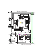
IC BLOCK DIAGRAM AND TERMINAL DESCRIPTIONS-21
Q1301: CXD2753R-5
No.
Pin Name
I/O
Pin Function
151
152
153
154
155
156
157
158
159
160
161
162
163
164
165
166
167
168
169
170
171
172
173
174
175
176
O
-
O
-
O
-
O
I
A9
A8
VDC
A7
A6
A5
A4
VSIO
A3
A2
A1
A0
VDIO
XSRQ
XSHD
SDCK
XSAK
SDEF
SD0
SD1
SD2
SD3
SD4
SD5
SD6
SD7
Address output terminal for SDRAM
Power supply terminal for core
Address output terminal for SDRAM
Ground terminal for I/O
Address output terminal for SDRAM
Address output terminal for SDRAM (LSB)
Power supply terminal for I/O
Data request output terminal to input into a front end processor
Input terminal of a header flag output by a front end processor
Input terminal of a data carrier clock output by a front end processor
Input terminal of data partial response flag output by a front end processor
Input terminal of error flag output by a front end processor
The stream data input terminal which is output by a front end processor (LSB)
The stream data input terminal which is output by a front end processor
The stream data input terminal which is output by a front end processor (MSB)
Ipu:Pull-up input, Ipd:Pull-down input, Ai:Analog input
www. xiaoyu163. com
QQ 376315150
9
9
2
8
9
4
2
9
8
TEL 13942296513
9
9
2
8
9
4
2
9
8
0
5
1
5
1
3
6
7
3
Q
Q
TEL 13942296513 QQ 376315150 892498299
TEL 13942296513 QQ 376315150 892498299


