


AR0331
15
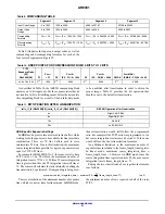
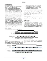
Figure 10. HiSPi Transmitter and Receiver Interface Block Diagram
A camera containing
the HiSPi transmitter
A host (DSP) containing
the HiSPi receiver
Dp0
Dn0
Dp1
Dn1
Dp2
Dn2
Dp3
Dn3
Cp0
Cn0
Tx
PHY0
Rx
PHY0
Dp0
Dn0
Dp1
Dn1
Dp2
Dn2
Dp3
Dn3
Cp0
Cn0
HiSPi Physical Layer
The HiSPi physical layer is partitioned into blocks of four
data lanes and an associated clock lane. Any reference to the
PHY in the remainder of this document is referring to this
minimum building block.
The PHY will serialize 10-, 12-, 14-, or 16-bit data words
and transmit each bit of data centered on a rising edge of the
clock, the second on the falling edge of the clock. Figure 11
shows bit transmission. In this example, the word is
transmitted in order of MSB to LSB. The receiver latches
data at the rising and falling edge of the clock.
Figure 11. Timing Diagram
cp
dn
…
…
MSB
LSB
TxPost
dp
cn
1 UI
TxPre
DLL Timing Adjustment
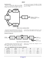
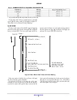
The specification includes a DLL to compensate for
differences in group delay for each data lane. The DLL is
connected to the clock lane and each data lane, which acts as
a control master for the output delay buffers. Once the DLL
has gained phase lock, each lane can be delayed in 1/8 unit
interval (UI) steps. This additional delay allows the user to
increase the setup or hold time at the receiver circuits and
can be used to compensate for skew introduced in PCB
design.
Delay compensation may be set for clock and/or data lines
in the hispi_timing register R0x31C0. If the DLL timing
adjustment is not required, the data and clock lane delay
settings should be set to a default code of 0x000 to reduce
jitter, skew, and power dissipation.
Figure 12. Block Diagram of DLL Timing Adjustment
delay
delay
del 1[2: 0]
delay
delay
del 3[2: 0]
delay
del 2[2: 0]
data _lane 0
data _lane 1
clock_lane0
delclock[2:0]
data_lane2
data_lane3
DA
TA0_DEL[2:0]