Octave Voyetra Eight Скачать руководство пользователя страница 11

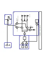
them on the MIXER CARD at the points called VOLUME L, R. The 
Master Volume Pot is routed to the JACK BAY for processing by the 
external Volume Pedal, and then routed to the MIXER CARD to the point 
labeled MASTER VOL. These control signals are multiplied by VCAs that 
convert them to control currents used to derive the volume/noise gate 
VCAs as illustrated on the schematic. 
 
The A440 tone comes from the DAC CARD and is turned off by the CPU. 
It is injected into the system audio by an inverter transistor designed to 
eliminate the digital noise that is present on all DAC CARD signals. 
 

2.3 Headphones 

The outputs of the VCA subchannel mixers are routed to another VCA, 
followed by an opamp used as a headphone driver. The front panel 
Headphone Volume control is used to send a control voltage to this VCA 
to set the headphone volume. 
 

2.4 Noise 

The noise source is generated by an MM5837 digital noise generator. 
This output is sent to two VCAs which set the noise L, R volume, and 
whose outputs are routed to the VCF cards L & R.  The noise is also 
passed through a low pass filter whose low frequency noise output is 
routed to the ANAMOD 1 CARD for use as a controller in the Modulation 
System. 
 

2.5 Calibrations 

Any VCA will have a certain amount of DC feedthrough from its control 
input to the output which causes an output signal that follows the DC 
control signal. This sounds like a “thumping” or “clicking” when fast attack 
and release ADSRs are used. To compensate for this, each VCA on the 
MIXER CARD has an offset adjustment trimmer which must be set for 
minimum DC feedthrough. This includes eight voice VCAs and two for 
the Left Right output VCAs. 
 
To assure that the voice volumes are all the same, individual channel 
volume trimmers are also adjusted. 
 

Содержание Voyetra Eight

Страница 1: ...By Reason 1 0 1984 Carmine J Bonanno Original Revision 1 0a 06 19 2002 Joan Touzet joant ieee org http www atypical net Mistake correction Revisions for clarity Started schematic entry Copywright sic...

Страница 2: ...10 2 3 HEADPHONES 11 2 4 NOISE 11 2 5 CALIBRATIONS 11 3 VCO CARD 12 3 1 THEORY OF OPERATION 12 3 2 VCO OPERATION 12 3 3 AUTOTUNE FUNCTIONALITY 13 3 4 DC VOLTAGES 14 3 5 CARD PIN SIGNALS 14 3 5 1 Input...

Страница 3: ...N SYSTEM SCAN CLOCKS 24 5 4 DEMULTIPLEXING REMULTIPLEXING 24 5 5 MONO CONTROLLER MULTIPLEXER 25 5 6 MISCELLANEOUS SWITCHING FUNCTIONS 25 6 KEYBOARD 26 6 1 THEORY OF OPERATION 26 6 2 CIRCUIT OPERATION...

Страница 4: ...pecific features Alternately the Quality Control Calibration test tape may be loaded into the instrument and the documented test procedure may be used to test all system functions for proper operation...

Страница 5: ...fer to the VCO section of this manual A strange clicking or thumping is heard whenever a key is pressed Is the click part of a patch Play the null patch and see if it goes away Try turning off the VCO...

Страница 6: ...tial filter resonance for each VCF 1 4 4 DAC Card Contains the Voice on off functions and the A D and D A functions which allow the CPU to control the analog system components Calibrations include DAC...

Страница 7: ...e jacks and an AGC circuit for the Tape input 1 4 12 Power Supply Contains regulators and fuses for 15V 5V 11V 22V as well as power down detection circuitry for the battery backed up RAM on the CPU 1...

Страница 8: ...w paths Mod Bank VCAs VCO1 VCO2 Fc Q 2 2 2 2 VCO1 VCO1 2 2 2 2 VCO2 VCO2 Mono Contr MIX VCO VCF VCO VCO VCF VCO DAC DIGI ANA1 ANA2 CPU POT x Press Mono Controllers Figure 1 2 Modulation System Signal...

Страница 9: ...8 8 8 VCA VCA VCA VCF Cards Phones Volume Phones Out 15 Noise Gen MM5837 VCA 2 Vol L R Right Mono Left Master Outputs Buffers VCA VCA Programmable CPU Vol L Parameter Trim Volume CPU Vol R Buffer Exte...

Страница 10: ...f two such that VCA 0 1 come from one op amp output VCA 2 3 from another op amp output and so on When the keyboard WHOLE 8 Mode is selected the output of sub mixer 0 1 is hard panned to one side of th...

Страница 11: ...control voltage to this VCA to set the headphone volume 2 4 Noise The noise source is generated by an MM5837 digital noise generator This output is sent to two VCAs which set the noise L R volume and...

Страница 12: ...te a square wave that is one octave below the oscillator frequency The waveforms are summed by an LF347 wide bandwidth op amp Since this summer is inverted it is followed by an inverter to form positi...

Страница 13: ...correction voltage it has to send to the VCO Control Input to have it generate a frequency of 440Hz when the middle A key is pressed on the keyboard This voltage is added to the keyboard voltage when...

Страница 14: ...oltages The card uses 15V to drive the CEM 3340s and opamp ICs The CEM 3340s also require a stable 5V reference which is derived on board to minimize system interaction between cards The 10V reference...

Страница 15: ...e CEM3340 3 6 3 Step 74 75 Linear FM Check Linear FM is when the output of the VCO2 mixer is routed to the linear control current input on VCO1 Problems can be caused by the CD4053 switch or if the ou...

Страница 16: ...an be caused by a bad CD4051 bad buffers or bad CEM3340 First switch the CD4051 with one on a voice that has no problems If the problem now appears on the other voice the CD4051 is bad Then try switch...

Страница 17: ...ents of the VCO volume VCAs and the noise voltage dropped across the 100K noise input resistors while the output current is converted to a voltage by the voltage to current converter opamp inverter TL...

Страница 18: ...tave change in filter frequency The control voltage is scaled down to less than 100mV at the SSM2044 input pin 13 to obtain the full sweep range of 20 Hz 20 kHz Filter resonance is determined by the c...

Страница 19: ...he LF347 buffer amplifiers that precede the CD4052 inputs prevent the scanning clocks from leaking into the VCF audio inputs 4 5 DC Voltages The card uses 15 Volts to drive the SSM ICs and associated...

Страница 20: ...n outputs from the CD4052 U7 and the four Fc modulation outputs should all be at 0 V Thus Q calibration problems where Q will not turn off should take this into account In steps 00 and 01 the Fc outpu...

Страница 21: ...and the associated TL068 buffers The outputs of all the TL068s should have a sweeping LFO sawtooth if they re functioning properly If not check if the CD4052 inputs pins 3 13 have sawtooths If they d...

Страница 22: ...ause the VCOs to jitter and sound unstable In this step the outputs of the TL068s are examined at a high scope sensitivity to weed out potentially bad ones The inputs to the CD4052s are all 0V so the...

Страница 23: ...s to address these demultiplexers so that the proper analog signal may be refreshed when necessary Since the system uses 15V to bias these CD4051s the control signals including address and enable vary...

Страница 24: ...by an M is encountered in the VOYETRA logic description e g MA0 it stands for modulation system signal Thus MA0 MA1 and MA2 are the modulation system address lines which are periodic square waves The...

Страница 25: ...witching Functions The two CD4174 addressable latches are used by the CPU to address the POT PANEL parameter trimmers See the POT PANEL theory for an explanation of how these trimmers are accessed The...

Страница 26: ...criptions in this section it would be best to review the POT PANTEL theory of operation since much of the explanations pertaining to the operation of the keyboard data and clock power lines is based o...

Страница 27: ...6 and latches all of the edge triggered CD4021s connected to the LATCH UB latch upper bus line when the gate transition from low to high occurs Since state Q1 on the CD4015 is still low the LOEWR BUS...

Страница 28: ...digital level translator CD4051 U8 and enables the analog multiplexer CD4051 U9 The ASTR also sets the outputs of the CD4024 divider to a low state addressing the first input of U9 which is the Y lin...

Страница 29: ...ressure sensors gain adjustment for left and right pressure sensors gain adjustment for left and right pressure sensors and balance Joystick calibrations include offset adjustment for X and Y axes and...

Страница 30: ...flip flop 74LS279 LOW When done the CPU writes to location 4 and sets the flip flop HIGH This DEMUXEN line drives a 16 channel demultiplexer on DIGIMOD that drives all of the system CD4051s In normal...

Страница 31: ...ators are driven by the unregulated 21V supply which is fused on the power supply board In normal operation the clock power line should always be active Since the CPU demands information from the keyb...

Страница 32: ...rther processed by the analog circuitry that follows the LM324 U16 buffers The CD4053 switches allow the VOYETRA to be controlled by a slave when they are switched to the external positions This is se...

Страница 33: ...ules Thus the trimmer diode network that follows the pitch bend buffer allows balance to be set while the gain controls for pitch bend left and right adjust for pitch bend range uniformity in both lef...

Отзывы: