


S32R274 EVB User Guide
9
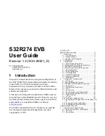
Figure 5.
Figure 5.
CAN DB9 connector pinout
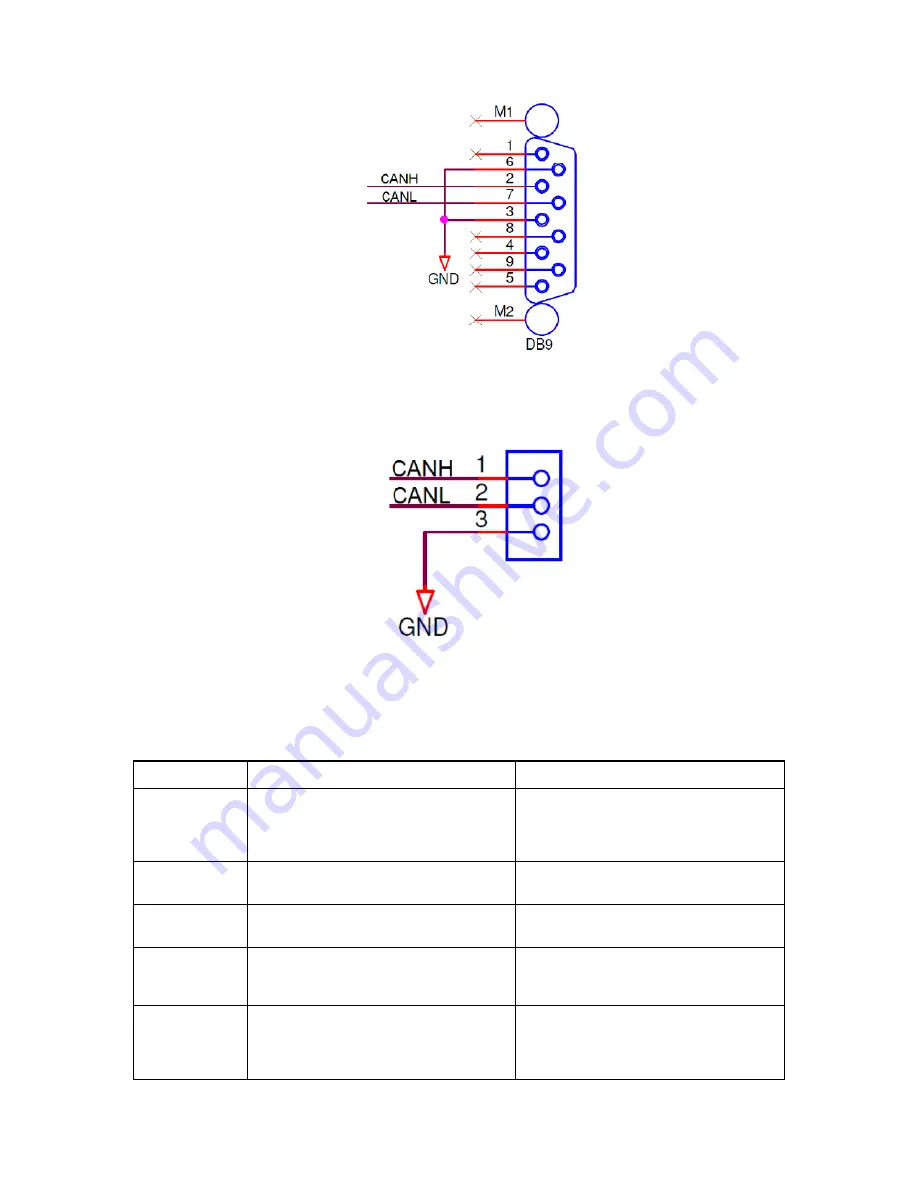
For flexibility, the CAN transceiver I/Os are also connected to two standard 0.1” connectors (P4 and P5)
at the top side of the PCB. The pin-out for these connectors is shown in Figure 6.
Figure 6.
Figure 6.
CAN 3pin header interface connector
By default the CAN interfaces are not enabled. To enable the CAN interfaces the jumpers detailed in
Table 3
need to be placed.
Table 3.
CAN control jumpers
Jumper
Label
Description
J23
CAN2_EN
PHY U2 configuration
1-2: WAKE to GND
3-4: STB to 5V
5-6: EN to 5V
J32
CAN2
1-2: PHY TX to MCU
3-4: PHY RX to MCU
J33
CAN-PWR
1-2: 5.0V_SR to PHY U2 V
CC
3-4: 12V to PHY U2 V
BAT
J34
-
PHY U2 signal out
1: ERR
2: INH
J21
CAN_EN
PHY U1 configuration
1-2: WAKE to GND
3-4: STB to 5V
5-6: EN to 5V