NXP Semiconductors S32K312EVB-Q172 Скачать руководство пользователя страница 18

NXP Semiconductors 


S32K312EVB-Q172 HWUM  


S32K312EVB-Q172 | S32K312EVBQ172ND - Hardware User Manual  


S32K312EVB-Q172  
S32K312EVBQ172ND 
HWUM 

All Information provided in this document is subject to legal disclaimers 

© NXP B.V. 2020. All rights reserved 

NXP Semiconductors 

REV A1 

– 01/2022 

Page 

18

 of 

25


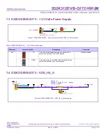
Table 10. CAN Interface - Connectors 

Connector 

Reference 

Circuit/ 

Interface 

Pin 

Number 

Signal/Connection 


J32 

CAN0 

CANH0 

CANL0 

GND 

NC 


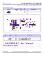
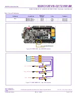
Figure 15. S32K312EVB-Q172 

– CAN Physical Layer0 - TJA1043 Secure HS-CAN Transceiver 


Table 11. CAN Interface 

– MCU Connections 

CAN


Interface 

Signal Name 

MCU 

Port 

Comment/Description 

TJA1153


/CAN0 

CAN0_RX 

PTA6 

[CAN0_RX Module] is routed to CAN Phy0 

CAN0_TX 

PTA7 

[CAN0_TX Module] is routed to CAN Phy0 

CAN0_ERRN 

PTC23 

PTC23 is routed to CAN Phy0 as CAN0_ERRN 

CAN0_EN 

PTC21 

PTC21 is routed to CAN Phy0 as CAN0_EN 

CAN0_STB 

PTC20 

PTC20 is routed to CAN Phy0 as CAN0_STB 


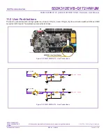
11  S32K312EVB-Q172 - User Peripherals 


11.1 User RGB LED Indicator 

There is 1 active high user RGB LEDs are connected by NPN transistors to the MCU ports. The USERLEDs are connected as follows: 


R532
10K

DNP

0402

R170
10K

DNP

0402

P5V0

R175
10K

0402

L4

BLM18KG121T Z1

1

2

C52
0.22UF

0402

C150
10uF
25V

CAN0_ERRN

Page[5]

VDD_HV_A_PERH

U13

PE

SD

2C

AN

1

2

3

R179

0 DNP

0402

L2

BLM18KG121T Z1

1

2

CAN0_STB

Page[5]

CAN0_ERRN

CAN0_INH

Page[3]

R3

0

0402

R166
60.4

CAN0_EN

Page[5]

J32
CON_1X4

CAN0_OUT

1
2
3
4

R199
60.4

CAN0_ERRN

C51
0.22UF

0402

C55
1UF

CAN0_INH

R203
10K

0402

TP94

TPAD

R204
10K

DNP

0402

TP39

TPAD

GND

CAN0_RX

Page[5]

C45

100pF

DNP
0402

C47
10uF

GND

CANH_OUT

Page[13]

C44
4700 PF

VBATP_CAN0

TJA1043

U34

TXD

1

G

N

D

2

VC

C

3

RXD

4

VI

O

5

EN

6

INH

7

ERR_N

8

WAKE

9

BAT

10

NC

11

CANL

12

CANH

13

STB

14

EPAD

15

TP95

TPAD

TP93

TPAD

CAN0_TX

Page[5]

CANL_OUT

Page[13]

R548

1.0K

R1

0

0402

R182
10K

0402

TP98

TPAD

TP36

TPAD

VBATP_SW

R196
10K

DNP

0402

C54

100pF

DNP
0402

R531
10K

0402

C151
0.22UF

0402

C145
0.22UF

0402

GND

TP96

TPAD

TP38

TPAD

CAN0_INH

Содержание S32K312EVB-Q172

Страница 1: ...S32K312EVB Q172 Customer Evaluation Board for S32K312 MCUs Hardware User Manual S32K312EVB Q172 S32K312EVBQ172ND...

Страница 2: ...7 S32K312EVB Q172 Power supply 8 7 1 S32K312EVB Q172 Main Power Supply 9 7 2 S32K312EVB Q172 5 0 Volts Power Supply 11 7 3 S32K312EVB Q172 3 3 Volts Power Supply 12 7 4 S32K312EVB Q172 VDD_HV_A 12 7...

Страница 3: ...rpose Input output GPO General Purpose Output I2C Inter Integrated Circuit ICE In Circuit Emulator I O Input output JTAG Joint Test Access Group LAN Local Area Network LCD Liquid Crystal Display LED L...

Страница 4: ...72 Block Diagram Figure 1 S32K312EVB Q172 Block diagram 4 S32K312EVB Q172 Features IMPORTANT Verify and download the last version of this document in http www nxp com Before the S32K312 Customer Evalu...

Страница 5: ...72 ND Reference Signal Default Configuration Description Comment S32K312 MCU U9 V1 01 P32K344EHT1VPBST MCU Power Supply VDD_HV_A_MCU 5 0V The VDDA_HV_A domain is connected to 5 0V Switching Power Supp...

Страница 6: ...IN Phy0 PTB10 LPUART9_TX is routed to LIN Phy0 LIN2 TJA1022T PTB28 LPUART5_RX is routed to LIN Phy1 PTB27 LPUART5_TX is routed to LIN Phy1 User Push Buttons SW4 Disabled Active Low SW5 PTB19 Active Lo...

Страница 7: ...subject to legal disclaimers NXP B V 2020 All rights reserved NXP Semiconductors REV A1 01 2022 Page 7 of 25 a The power switch SW1 must be in OFF position before to the EVB be connected to an externa...

Страница 8: ...B Q172 Power supply Input and LED power indicators If no LED s are illuminated when power is applied to the EVB and the regulators are correctly enabled using the appropriate jumpers it is possible th...

Страница 9: ...emiconductors REV A1 01 2022 Page 9 of 25 7 1 S32K312EVB Q172 Main Power Supply Figure 4 S32K312EVB Q172 Main power supply input Table 2 Main power supply connector Connector Description Ground V 12Vo...

Страница 10: ...bled and can be used during customer production process to flash MCU without need of WD refresh After 80ms once the SW1 is in ON position the VDEBUG pin will be switching to a low voltage GND due to t...

Страница 11: ...atchdog refresh by SPI Please review the FS26 documentation J5 OPEN All change of jumpers must be done once the EVB is unpowered from J3 and J5 as MANDATORY 7 2 S32K312EVB Q172 5 0 Volts Power Supply...

Страница 12: ...upply Reference Jumper Position Description Comments J26 1 2 The 3 3V Switching power supply is routed to the main P3V3 domain 3 3V for all board Default closed OPEN The 3 3V output of the FS26x SBC i...

Страница 13: ...3 P3V3 3 3V from the FS26 is selected for the VDD_HV_A_MCU reference OPEN VDD_HV_A domain is isolated and unpowered J10 1 2 VDD_HV_A is routed to VDD_HV_A_MCU reference This jumper can be used to cur...

Страница 14: ...tors REV A1 01 2022 Page 14 of 25 8 S32K312EVB Q172 Programming and Debug Interface 8 1 RESET Switch and LED indicator The RESET switch SW2 provides for manual application of the RESET input signal Th...

Страница 15: ...50 This small 20 pin 0 05 connector provides access to SWD SWV JTAG and ETM 4 bit signals available on a Cortex M3 M4 M7 device A 20 pin header Samtec FTSH 110 01 is specified with dimensions 0 50 x 0...

Страница 16: ...72 LIN Interface The EVB incorporates two LIN interfaces connected the S32K312 MCU Using an NXP LIN transceivers the TJA1021T 20 C supporting both master and slave mode jumper selectable The output fr...

Страница 17: ...AN Interface Figure 14 S32K312EVB Q172 CAN Interface LIN2_OUT Page 13 VBATP_SW VDD_HV_B_PERH LIN1_SLP D17 PMEG4050EP A C LIN1_OUT Page 13 LIN Connector D8 PESD1LIN 1 2 VBATLIN1_TJA1021 D10 PESD1LIN 1...

Страница 18: ...to CAN Phy0 as CAN0_STB 11 S32K312EVB Q172 User Peripherals 11 1 User RGB LED Indicator There is 1 active high user RGB LEDs are connected by NPN transistors to the MCU ports The USERLEDs are connecte...

Страница 19: ...ault Color Comment D13 RGBLED0_RED PTA29 Red Active High RGBLED0_GREEN PTA30 Green Active High RGBLED0_BLUE PTA31 Blue Active High Figure 16 S32K312EVB User RGB LED Indicator Figure 17 S32K312EVB Q172...

Страница 20: ...uttons active to high pulled low driven to VDD_HV_A and VDD_HV_B the push button switches SW6 and SW5 connected to MCU ports The switches are connected as follows Figure 18 S32K312EVB Q172 User Pushbu...

Страница 21: ...ween each USER_SWx and the MCU pins These can be removed if required to isolate or change the User Switch from the default MCU pin 11 3 ADC Rotary Potentiometers The EVB incorporates a couple of ADC R...

Страница 22: ...o legal disclaimers NXP B V 2020 All rights reserved NXP Semiconductors REV A1 01 2022 Page 22 of 25 Figure 21 S32K312EVB Q172 ADC Rotary Potentiometers 12 S32K312EVB Q172 Default Jumpers Figure 22 S3...

Страница 23: ...ion Description Comments FS26x SBC Power Supply J22 1 2 FS26_VLDO1 5 0V is routed to P5V0 domain J26 1 2 FS26_VLDO2 3 3V is routed to P3V3 domain J1 1 2 Flash Mode configuration in the FS26 J5 1 2 S32...

Страница 24: ...ation provided in this document is subject to legal disclaimers NXP B V 2020 All rights reserved NXP Semiconductors REV A1 01 2022 Page 24 of 25 13 S32K312EVB Q172 Revision history Table 16 Revision h...

Страница 25: ...pts no liability for any assistance with applications or customer product design It is customer s sole responsibility to determine whether the NXP Semiconductors product is suitable and fit for the cu...

Отзывы: