


NXP Semiconductors
S32K312EVB-Q172 HWUM
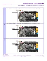
S32K312EVB-Q172 | S32K312EVBQ172ND - Hardware User Manual
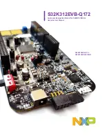
S32K312EVB-Q172
S32K312EVBQ172ND
HWUM
All Information provided in this document is subject to legal disclaimers
© NXP B.V. 2020. All rights reserved
NXP Semiconductors
REV A1
– 01/2022
Page
11
of
25
Reference
Jumper Position
Description
Comments
Normal Mode
J1
OPEN
In this mode the FS26 can enter Normal mode by configuring the
init_fs window and sending properly serviced watchdog refresh
by SPI. Please review the FS26 documentation.
J5
OPEN
All change of jumpers must be done once the EVB is unpowered from J3 and J5 as MANDATORY
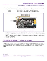
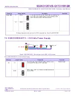
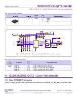
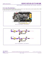
7.2 S32K312EVB-Q172
– +5.0 Volts Power Supply
Figure 6. S32K312EVB-Q172
– General jumper for the P5V0 (+5.0V) reference
Table 4. S32K312EVB-Q172
– +5.0 Volts Power Supply
Reference
Jumper Position
Description
Comments
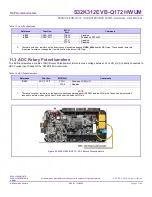
J22
1-2
The +5.0V output of the FS26x SBC [FS26_VLDO1] is routed
to the main P5V0 domain (+5.0V for all board).
Default closed
OPEN
P5V0 domain (+5.0V for all board) is isolated/disconnected
from the FS26x
P5V0
J22
HDR 1X3
SILK = P5V0
JUMPER(Default) = 1-2
1
2
3
TP26
SILK = P5V0
1
5V0 OUTPUT
FS26_VLDO1
P5V0_OSDA_OUT