
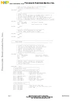


A
A
B
B
C
C
D
D
E
E
4
4
3
3
2
2
1
1
64Mb
128Mb
256Mb
SDRAM CLOC
K
TERMINATIO
N
Memory
Am29LV640DU/Am29LV641DU
Am29DL322C/Am29DL323C
Am29LV160B/MBM29LV160
Am29LV800B
INSTALL
INSTALL
INSTALL
INSTALL
NOT
PLACED
R4, R5, R6
R4, R5, R6, R7
DEFAULT
R4, R5
R4, R5, R7, R8, R9
*
*
*
Am29LV640DU/Am29LV641DU
Am29DL322C/Am29DL323C
Am29LV160B/MBM29LV160
Am29LV800B
INSTALL
INSTALL
INSTALL
INSTALL
R12, R14, R15, R17
DEFAULT
R12, R14
R12, R14, R17, R18, R19
*
*
*
R12, R14, R15
DEFAULT INSTALLED
VZADS10.DSN
1.0
VZ ADS Board
2 Dai King Street, Tai Po Industrial Estate, Tai Po, NT,
Hong
Kong.
B
31
1
Tuesday, November 09, 1999
Title
S
iz
e
Document Number
R
e
v
Date:
Sheet
of
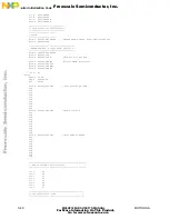
D7
A21
A12
A5
A10
A16
A4
A17
D8
D0
D15
A8
A18
D1
D3
D6
A20
A14
D11
A13
A15
A1
A3
A9
A0
A7
A19
D13
D2
D10
A6
D5
A11
D4
D9
A2
D14
D12
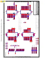
A13
BS0
BS1
SDA11
A13
A12
A13
A12
A15
A14
BS1
SDA11
BS0
BS1
BS0
SDA11
SDA12
A12
A15
A16
D6
A9
A6
D15
D9
A5
SDCE
SDCLK
A2
BS1
DQML
D0
BS0
A1
SDA12
SDA11
A8
DQMH
D13
SDA10
~SDRAS
A7
D3
D10
~SDCS1
D5
D4
A10
D7
D8
D14
~SDWE
A3
D1
D12
D11
~SDCAS
D2
A4
SDCLK
A[0..23]
D[0..15]
D6
A9
A6
D15
D9
A5
SDCE
SDCLK
A2
BS1
DQML
D0
BS0
A1
SDA12
SDA11
A8
DQMH
D13
SDA10
~SDRAS
A7
D3
D10
~SDCS0
D5
D4
A10
D7
D8
D14
~SDWE
A3
D1
D12
D11
~SDCAS
D2
A4
D0
D1
D2
D3
D4
D5
D6
D7
D8
D9
D10
D11
D12
D13
D15
D14
A20
A1
A2
A3
A4
A5
A6
A7
A8
A9
A10
A11
A12
A13
A14
A15
A16
A17
A18
A19
A21
~FLASH0
~OE
~WE
A20
A22
D0
D1
D2
D3
D4
D5
D6
D7
D8
D9
D10
D11
D12
D13
D15
D14
A20
A1
A2
A3
A4
A5
A6
A7
A8
A9
A10
A11
A12
A13
A14
A15
A16
A17
A18
A19
A21
~FLASH1
~OE
~WE
A20
A22
A22
VCC
VCC
VCC
VCC
VCC
VCC
VCC
VCC
VCC
VCC
VCC
VCC
VCC
VCC
VCC
VCC
VCC
VCC
VCC
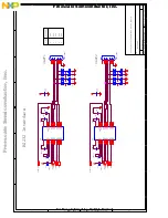
R6
000
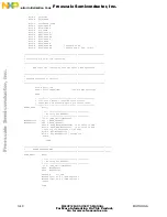
54 pins
16-bit SDRA
M
Size:64Mb,
128Mb,256M
b
TSOP(II)
U4
SDRAM
VC
C
1
DQ0
2
GN
D
6
DQ1
4
VC
C
3
DQ2
5
GN
D
52
DQ3
7
VC
C
9
LDQM
15
WE
16
A11
35
A10/AP
22
A0
23
A1
24
A2
25
A3
26
VC
C
14
GN
D
46
A4
29
A5
30
A6
31
A7
32
A8
33
A9
34
VC
C
49
DQ4
8
GN
D
41
DQ5
10
VC
C
27
DQ6
11
GN
D
28
DQ7
13
GN
D
12
BS1
21
BS0
20
A12/NC
36
NC
40
GN
D
54
VC
C
43
DQ8
42
DQ9
44
DQ10
45
DQ11
47
DQ12
48
DQ13
50
DQ14
51
DQ15
53
CKE
37
CLK
38
CS
19
RAS
18
CAS
17
UDQM
39
R8
000
TSOP (I)
U3
FLASH
DQ1
31
DQ2
33
DQ3
35
DQ4
38
DQ5
40
DQ6
42
DQ7
44
DQ8
30
DQ9
32
DQ0
29
DQ10
34
DQ11
36
DQ12
39
DQ13
41
DQ14
43
DQ15/A-1
45
A0
25
A1
24
A2
23
A3
22
A4
21
A5
20
A6
19
A7
18
A8
8
A9
7
A10
6
A11
5
A12
4
A13
3
A14
2
A15
1
A16
48
WE
11
OE
28
CE
26
RY/BY
15
BYTE
47
VC
C
37
VS
S
27
VS
S
46
A17
17
A18
16
RESET
12
A19
9
A20
10
WP/ACC
14
NC
13
R4
4K7
R7
4K7
R5
4K7
R9
000
R22
000
R21
000
R20
000
R16
000
R13
000
R11
000
R26
000
R25
000
R24
000
R23
000
C27
0.1u
54 pins
16-bit SDRA
M
Size:64Mb,
128Mb,256M
b
TSOP(II)
U5
SDRAM
VC
C
1
DQ0
2
GN
D
6
DQ1
4
VC
C
3
DQ2
5
GN
D
52
DQ3
7
VC
C
9
LDQM
15
WE
16
A11
35
A10/AP
22
A0
23
A1
24
A2
25
A3
26
VC
C
14
GN
D
46
A4
29
A5
30
A6
31
A7
32
A8
33
A9
34
VC
C
49
DQ4
8
GN
D
41
DQ5
10
VC
C
27
DQ6
11
GN
D
28
DQ7
13
GN
D
12
BS1
21
BS0
20
A12/NC
36
NC
40
GN
D
54
VC
C
43
DQ8
42
DQ9
44
DQ10
45
DQ11
47
DQ12
48
DQ13
50
DQ14
51
DQ15
53
CKE
37
CLK
38
CS
19
RAS
18
CAS
17
UDQM
39
C24
0.1u
C23
0.1u
R3
200
C29
0.01u
R10
200
C28
0.01u
C34
0.1u
C33
0.1u
C32
0.1u
C31
0.1u
C26
0.1u
C25
0.1u
R15
000
R18
000
TSOP (I)
U6
FLASH
DQ1
31
DQ2
33
DQ3
35
DQ4
38
DQ5
40
DQ6
42
DQ7
44
DQ8
30
DQ9
32
DQ0
29
DQ10
34
DQ11
36
DQ12
39
DQ13
41
DQ14
43
DQ15/A-1
45
A0
25
A1
24
A2
23
A3
22
A4
21
A5
20
A6
19
A7
18
A8
8
A9
7
A10
6
A11
5
A12
4
A13
3
A14
2
A15
1
A16
48
WE
11
OE
28
CE
26
RY/BY
15
BYTE
47
VC
C
37
VS
S
27
VS
S
46
A17
17
A18
16
RESET
12
A19
9
A20
10
WP/ACC
14
NC
13
R12
4K7
R17
4K7
R14
4K7
R19
000
C30
0.1u
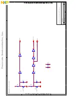
A[0..23]
D[0..15]
SDA10
SDA11
SDA12
BS0
BS1
DQML
DQMH
SDCE
SDCLK
~SDCS1
~SDRAS
~SDCAS
~SDWE
SDA10
SDA11
SDA12
BS0
BS1
DQML
DQMH
SDCE
SDCLK
~SDCS0
~SDRAS
~SDCAS
~SDWE
~OE
~WE
~OE
~WE
~FLASH0
~FLASH1
Freescale Semiconductor, I
Freescale Semiconductor, Inc.
For More Information On This Product,
Go to: www.freescale.com
nc.
..